10–112 GBPS READY

High-Speed PCB Manufacturing — Low-Loss, Backdrill, VIPPO

Low-loss stackups, VLP copper, and precision via processing keep 10–112 Gbps SERDES, PCIe Gen5/6, and PAM4 links within eye margins from prototype to production.

  • Megtron / Tachyon / I-Speed
  • VLP / HVLP copper control
  • Backdrill + VIPPO
  • ±5% impedance coupons
  • 7-day quick-turn SI builds
  • TDR + VNA reports

Get an Instant Quote

Full Quote →

High-Speed PCB Fabrication & Assembly

APTPCB engineers interpret SI requirements, map stackups, and lock dielectric spacing, copper roughness, and resin content to preserve insertion loss budgets.

We coordinate backdrill depths, via-in-pad plated over, and reference plane management before fabrication, then run TDR coupons and optional VNA sweeps for each lot.

Cleanroom SMT with press-fit tooling, stiffeners, and handling instructions keeps BGA escapes, high-layer cores, and cage/connector soldering aligned with compliance tests.

APTPCB's high-speed design rule states that whenever rise time approaches four times the propagation delay (Tr < 4×tp) or data rates exceed 1 Gbps, the interconnect must be modeled as a transmission line. We apply that criterion early so stack-ups, dielectrics, and routing styles are locked before layout proceeds.

Our guide differentiates high-speed digital and high-frequency analog behavior, listing common pitfalls such as reflections, impedance discontinuities, EMI, and thermal constraints. We keep that checklist on every Altium/KiCad review so plane references, decoupling, and routing rules are optimized from day one.

High-speed PCB manufacturing lab

High-Speed Programs Delivered

Representative builds across data center, automotive, telecom, aerospace, and test equipment.

112G data center blades

112G data center blades

Automotive sensor fusion

Automotive sensor fusion

5G/6G radio heads

5G/6G radio heads

Aerospace comms modules

Aerospace comms modules

Test & measurement backplanes

Test & measurement backplanes

AI/accelerator interposers

AI/accelerator interposers

High-Speed Reliability & SI Compliance

Stackups include differential pair coupons, backdrill depth logs, and SI data, ensuring each lot holds insertion loss, skew, and impedance targets.

Download Capabilities
Df ≤0.0015 laminatesVLP copper optionsBackdrill + VIPPOImpedance ±5% couponsTDR + VNA reporting7-day quick-turn

APTPCB High-Speed PCB Services

We deliver low-loss stackups, SI documentation, and manufacturing discipline for SERDES, PAM4, and RF/microwave systems.

High-Speed PCB Types

Choose between hybrid FR-4/low-loss builds, full low-Df stacks, backplanes, or rigid-flex high-speed harness replacements.

  • Hybrid High-Speed Multilayer – Low-loss cores near SERDES layers with FR-4 elsewhere to control cost.
  • Full Low-Loss Stackups – Megtron, Tachyon, or I-Speed throughout for 56–112 Gbps leaf-spine builds.
  • Backplane & Midplane – 20+ layer stacks with dual backdrill, press-fit connectors, and heavy copper planes.
  • High-Speed Rigid-Flex – Flex tails carry high-speed links between rigid sections for compact enclosures.
  • RF/Microwave Hybrids – PTFE or hydrocarbon cores near antennas, FR-4 for logic and power sections.

Via, Launch & Transition Control

  • Backdrilled PTH: Remove via stubs feeding SERDES channels to reduce reflections.
  • VIPPO: Via-in-pad plated over for fine-pitch BGAs, minimizing inductance at launches.
  • Stacked / Staggered Microvias: Connect dense BGA layers without adding stubs.
  • Resin-Coated Copper (RCC) Cores: Ultra-thin cores that keep dielectric spacing constant.
  • Embedded Edge Launches: Controlled transitions to coax or SMPM connectors.
  • Skived Ground Returns: Maintain short return paths under differential pairs.

Sample High-Speed Stackups

  • 14L Hybrid: Megtron 6 signal pairs on L2/L13 with FR-4 cores for power distribution.
  • 20L Backplane: Dual stripline groups, dual backdrill operations, and press-fit connector zones.
  • High-Speed Rigid-Flex: 8L rigid core with 2 flex tails carrying PCIe Gen5 links between modules.

Material & Design Guidelines

Pair low-Df cores with HVLP copper, control resin content, and maintain symmetric stacks to mitigate skew and warpage.

  • Specify dielectric constant and dissipation factor per layer to control delay and loss.
  • Use VLP or HVLP copper to reduce conductor loss while balancing cost.
  • Maintain consistent dielectric thickness to hold impedance within ±5%.
  • Avoid plane splits under differential pairs; provide return vias near transitions.

Reliability & SI Validation

Insertion loss, skew, eye height, and impedance are verified via coupons, TDR, and optional VNA sweeps before shipment.

Cost & Application Guidance

  • Hybrid stackups: Use low-loss laminates only on critical layers to control BOM.
  • Backplane builds: Consolidate press-fit connectors and share drill hits to reduce costs.
  • Quick-turn SI prototypes: Standardize layer counts and materials for faster quoting and lower NRE.

High-Speed PCB Manufacturing Flow

1

Stackup & SI Review

Align loss budgets, dielectric targets, and via strategy before tooling.

2

Imaging & Drill

3/3 mil LDI, controlled depth drilling, and laser microvias for dense escapes.

3

Copper & Lamination

HVLP copper prep, symmetric lamination, and copper balancing for low skew.

4

Backdrill & VIPPO

CNC backdrill, via fill, and planarization to remove stubs and prep for assembly.

5

Assembly & Test

Press-fit connectors, cleanroom SMT, and fixture-based testing.

6

SI Validation

TDR, S-parameter, and eye diagram verification with documented reports.

7

Transmission-Line Modeling

Use the APTPCB criterion to run TDR/simulation on nets whose Tr approaches propagation delay, then lock impedance, dielectric constants, and differential spacing.

8

EMI & Return-Path Review

Walk the EMI checklist to confirm reference planes, via stitching, terminations, and return paths keep reflections and crosstalk within budget.

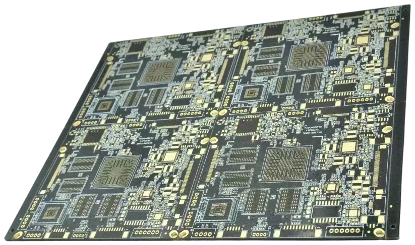
High-Speed CAM & SI Coordination

CAM engineers translate SI constraints into manufacturing files, defining stackups, drill maps, impedance coupons, and backdrill coordinates.

  • Document dielectric targets, copper roughness, and resin content per layer.
  • Define impedance coupons, differential pair geometries, and tolerance stackups.
  • Plan backdrill depths, VIPPO fills, and reference plane stitching vias.
  • Coordinate press-fit connector footprints and tear-drop requirements.
  • Simulate or validate via transitions with SI tool outputs.
  • Provide handling and baking instructions for low-loss materials.
  • Release fabrication notes detailing allowed substitutions and QC checkpoints.

Manufacturing Execution & SI Feedback

Process engineers control lamination, drilling, plating, and measurement data, feeding SI metrics back to CAM and design teams.

  • Monitor lamination temperature/pressure to prevent dielectric shift.
  • Measure copper roughness and dielectric thickness to confirm stackup targets.
  • Inspect drill accuracy, via plating, and backdrill depth per lot.
  • Validate VIPPO planarity before SMT.
  • Run TDR/VNA tests on coupons; archive reports.
  • Package boards with moisture control and SI documentation.
10–112 Gbps

SERDES Data Rate

PCIe Gen5/6, PAM4, Ethernet

Df ≤0.0015

Dielectric Loss

Megtron / Tachyon class materials

±5%

Impedance Tolerance

Differential coupons per lot

0.5 ns/cm

Propagation Delay

Controlled dielectric spacing

Advantages of High-Speed PCBs

Maintain signal integrity, reduce loss, and accelerate compliance.

Validated SI Performance

Each lot includes impedance coupons and optional S-parameter data.

Tailored Stackups

Hybrid low-loss stackups balance cost and performance.

Precise Via Control

Backdrill, VIPPO, and microvia strategies remove stubs and inductance.

Reliability Under Stress

Thermal, vibration, and humidity testing ensure links stay stable.

System-Level Savings

Optimized routing reduces re-spins and compliance risk.

Compliance Documentation

Comprehensive SI reports accompany every shipment.

Why Choose APTPCB?

Proper stackups, materials, and via transitions keep SERDES and RF designs within eye diagram targets while controlling cost.

Data centerTelecomAutomotiveAerospaceIndustrial testAI hardware
APTPCB production line
Low-loss PCB line • Backdrill & VIPPO • SI reporting per lot

High-Speed PCB Applications

Where low loss, tight impedance, and SI validation are non-negotiable.

Data center blades, automotive ADAS, telecom radios, aerospace comms, and industrial instrumentation all rely on disciplined stackups.

Data Center & AI

112G leaf-spine fabrics, SmartNICs, and accelerator boards.

Leaf-spineSmartNICAcceleratorsStorageSwitch

Automotive & ADAS

Sensor fusion, radar, and autonomy controllers with high-speed interconnects.

ADASRadarSensor fusionInfotainmentBattery

Telecom & 5G/6G

Massive MIMO radios, fronthaul/backhaul, and optical transport.

RRUBTSOpticalMicrowaveIoT hubs

Aerospace & Defense

High-speed communications, radar, EW, and avionics modules.

AvionicsEWRadarSatcomISR

Industrial & Test

Measurement equipment, oscilloscopes, and inspection tools.

OscilloscopesATEInspectionFactory IoTMetrology

Instrumentation & RF Labs

RF/microwave instruments and research platforms.

RF labsSpectrumNetwork analyzersPrototypingLabs

Consumer & Prosumer

Gaming consoles, VR headsets, and creator gear with high-speed buses.

VRConsolesCamerasAudioCreators

Rigid-Flex Harness

Compact modules combining high-speed rigid cores with flex jumpers.

Rigid-flexModulesWearablesEdge devicesIoT

High-Speed Design Challenges & Solutions

Stackup, via, and SI control are essential to keep SERDES eye diagrams open.

Common Design Challenges

01

Insertion Loss Budgets

Inconsistent laminates or copper roughness increases IL and shrinks eye height.

02

Via Stub Reflections

Poor backdrill or blind via planning produces reflections and resonances.

03

Skew & Timing

Mismatched dielectric thickness or routing lengths upset skew budgets.

04

Crosstalk & EMI

Improper spacing, reference plane splits, or return path gaps raise crosstalk.

05

Thermal & Mechanical Stress

Dense copper and high layer counts need balanced lamination to avoid warpage.

06

Compliance Documentation

Incomplete SI data slows regulatory or interoperability approval.

Our Engineering Solutions

01

Material & Stackup Modeling

We simulate dielectric, copper roughness, and lamination stack to match IL/Dk targets.

02

Via Strategy & Backdrill Planning

Define backdrill lengths, VIPPO fills, and return vias to remove resonances.

03

Differential Pair Governance

Controlled spacing, guard traces, and stitching via rules keep crosstalk down.

04

Thermal Relief & Balancing

Copper balancing and step lamination mitigate warpage in 20+ layer builds.

05

SI Test Packages

Coupons, fixtures, and documentation flow directly into your compliance archive.

How to Control High-Speed PCB Cost

Low-loss materials and complex drill steps raise cost—apply them only where SI demands. Standardizing layer counts and stackups shortens quoting and keeps quick-turn runs affordable. Share SI requirements, connector types, and compliance targets early so we can map the simplest viable stackup.

01 / 08

Hybridize Materials

Use low-loss cores only on SERDES layers, FR-4 elsewhere.

02 / 08

Specify Copper Roughness

Choose VLP grades that meet SI needs without overpaying for HVLP everywhere.

03 / 08

Align Surface Finish

ENIG suits most high-speed builds; specify ENEPIG only for mixed wire bond.

04 / 08

Optimize Backdrill Steps

Group vias by depth to reduce drill time and tooling.

05 / 08

Define Testing Scope

Target essential SI tests per lot; reserve full VNA sweeps for qualification.

06 / 08

Early DFx with SI Team

Joint reviews reduce respins and expedite compliance approvals.

07 / 08

Standardize Stackups

Reuse proven layer counts to avoid new tooling and faster quoting.

08 / 08

Coordinate Press-Fit Connectors

Align connector selection with available drill hits to limit NRE.

Certifications & Standards

Quality, environmental, and industry credentials supporting reliable manufacturing.

Certification
ISO 9001:2015

Quality management for high-speed fabrication.

Certification
ISO 14001:2015

Process controls for copper and lamination.

Certification
ISO 13485:2016

Traceability for medical & instrumentation SI builds.

Certification
IATF 16949

Automotive SI documentation for ADAS links.

Certification
AS9100

Aerospace-grade governance for high-speed interconnects.

Certification
IPC-6012 / 6013

Performance classes for rigid and rigid-flex.

Certification
UL 94 V-0 / UL 796

Flammability and dielectric safety.

Certification
RoHS / REACH

Hazardous substance compliance.

Selecting a High-Speed PCB Partner

  • Low-loss laminate supply with traceability.
  • Backdrill, VIPPO, and laser microvia capability in-house.
  • SI engineers providing TDR/VNA reports under NDAs.
  • Cleanroom SMT with press-fit tooling and inspection.
  • Quick-turn capacity with replicated processes for production.
  • Bilingual engineering support and 24-hour DFx feedback.
Engineers reviewing SI reports

Quality & Cost Console

Process & Reliability Controls + Economic Levers

Unified dashboard connecting HDI quality checkpoints with the economic levers that compress cost.

Process & Reliability

Pre-Lamination Controls

Stack-Up Validation

  • Panel utilization+5–8%
  • Stack-up simulation±2% thickness
  • VIPPO planningPer lot
  • Material bake110 °C vacuum

Pre-Lamination Strategy

• Rotate outlines, mirror flex tails

• Share coupons across programs

• Reclaim 5-8% panel area

Registration

Laser & Metrology

Registration

  • Laser drill accuracy±12 μm
  • Microvia aspect ratio≤ 1:1
  • Coverlay alignment±0.05 mm
  • AOI overlaySPC logged

Laser Metrology

• Online laser capture

• ±0.05 mm tolerance band

• Auto-logged to SPC

Testing

Electrical & Reliability

Testing

  • Impedance & TDR±5% tolerance
  • Insertion lossLow-loss verified
  • Skew testingDifferential pairs
  • Microvia reliability> 1000 cycles

Electrical Test

• TDR coupons per panel

• IPC-6013 Class 3

• Force-resistance drift logged

Integration

Assembly Interfaces

Integration

  • Cleanroom SMTCarrier + ESD
  • Moisture control≤ 0.1% RH
  • Selective materialsLCP / low Df only where needed
  • ECN governanceVersion-controlled

Assembly Controls

• Nitrogen reflow

• Inline plasma clean

• 48h logistics consolidation

Architecture

Stack-Up Economics

Architecture

  • Lamination cyclesOptimize 1+N+1/2+N+2
  • Hybrid materialsLow-loss where required
  • Copper weightsMix 0.5/1 oz strategically
  • BOM alignmentStandard cores first

Cost Strategy

• Balance cost vs performance

• Standardize on common cores

• Low-loss only on RF layers

Microvia Planning

Via Strategy

Microvia Planning

  • Staggered over stacked-18% cost
  • Backdrill sharingCommon depths
  • Buried via reuseAcross nets
  • Fill specificationOnly for VIPPO

Via Cost Savings

• Avoid stacked microvias

• Share backdrill tools

• Minimize fill costs

Utilization

Panel Efficiency

Utilization

  • Outline rotation+4–6% yield
  • Shared couponsMulti-program
  • Coupon placementEdge pooled
  • Tooling commonalityPanel families

Panel Optimization

• Rotate for nesting efficiency

• Share test coupons

• Standardize tooling

Execution

Supply Chain & Coating

Execution

  • Material poolingMonthly ladder
  • Dual-source PPAPPre-qualified
  • Selective finishENIG / OSP mix
  • Logistics lanes48 h consolidation

Supply Chain Levers

• Pool low-loss material

• Dual-source laminates

• Match finish to need

High-Speed PCB Manufacturing — Upload Data for SI Review

Talk to SI Engineers
IPC-6012/6018 compliance
SI reporting included
Low-loss stackup expertise
Prototype-to-production continuity

Share stackups, connector maps, and compliance targets — we respond with DFx notes, SI data scope, and lead time within one business day.

High-Speed PCB FAQ

Common questions about materials, impedance, and SI validation.