Precision vacuum hydraulic lamination press and multilayer PCB stack-up

Structural Integrity Control

Advanced PCB Lamination & Multilayer Stack-Up Manufacturing Services

The structural core of any highly reliable printed circuit board is its lamination integrity. APTPCB provides precision vacuum hydraulic pressing and sequential lamination services for complex multilayer architectures up to 64 layers. We specialize in hybrid PTFE / FR-4 bonding, high-Tg resin encapsulation for heavy copper, and multi-cycle HDI press sequences governed by thermocouple-monitored cure profiles.

4 to 64
Layer Counts
Any-Layer
Sequential Lamination
Hybrid
PTFE + FR-4 Bonding

Get an Instant Quote

Sequential LaminationHDI Blind / Buried Vias
Hybrid Stack-UpsPTFE + FR-4 Integration
Thermocouple ControlPrecision Cure Profiles
Vacuum HydraulicVoid-Free Encapsulation
X-Ray AlignmentSub-mil Registration
CTE ManagementWarpage Prevention
ISO 9001 / IATFQuality Certified
IPC Class 3Defense Standard
Sequential LaminationHDI Blind / Buried Vias
Hybrid Stack-UpsPTFE + FR-4 Integration
Thermocouple ControlPrecision Cure Profiles
Vacuum HydraulicVoid-Free Encapsulation
X-Ray AlignmentSub-mil Registration
CTE ManagementWarpage Prevention
ISO 9001 / IATFQuality Certified
IPC Class 3Defense Standard

Precision Structural Fabrication

Precision Lamination Technology for High-Reliability Global Electronics

The foundation of every robust multilayer board lies inside the lamination press. APTPCB provides advanced pressing and sequential lamination services for complex designs deployed by hardware innovators from Silicon Valley tech hubs to manufacturing centers in Tokyo. When dealing with extreme routing densities or high-power electronics, improper lamination inevitably leads to catastrophic failures—such as resin starvation, internal micro-delamination, or severe board warpage during the SMT assembly reflow cycle.

From manufacturing 32-layer AI accelerator backplanes to fabricating hybrid radar modules for European Tier-1 automotive suppliers, our process transcends simply applying heat and pressure. We utilize state-of-the-art vacuum hydraulic presses governed by customized cure profiles tailored specifically to your chosen stack-up design and resin system. Whether bonding ultra-low-loss Megtron 6 cores, executing hybrid Rogers/FR-4 constructions, or flowing high-resin prepregs around 6 oz heavy copper, our process ensures exact dielectric thickness control, completely void-free resin fill, and perfectly symmetrical CTE (Coefficient of Thermal Expansion) balancing for extreme environmental survival.

Hybrid multilayer PCB microsection showing PTFE and FR-4 lamination integrity

Lamination Capabilities

Advanced Lamination & Pressing Specifications

Different materials and architectures demand drastically different thermodynamic press cycles. Below are our validated lamination capabilities for high-performance interconnects.

Lamination ProcessSupported MaterialsPrimary ApplicationKey Manufacturing Controls
Single-Press MultilayerStandard & High-Tg FR-4, Halogen-FreeStandard 4 to 16-layer boards with mechanical through-holes.Optimized heat ramp rates to ensure complete B-stage resin flow before final thermoset curing.
Sequential Lamination (HDI)Isola 370HR, I-Tera, Panasonic MegtronAny-Layer HDI, designs requiring blind/buried microvias (e.g., 3+N+3).Multiple high-heat press cycles requiring extreme X-ray registration control to prevent inner layer shifting.
Hybrid Stack-Up LaminationRogers RO4000/RO3000 + FR-4, Taconic + FR-4Cost-optimized RF/Microwave boards, automotive radar, 5G base stations.Careful management of differing Z-axis CTEs. Utilizing specialized low-flow bonding prepregs (e.g., RO4450F).
Heavy Copper EncapsulationHigh-Tg FR-4, PolyimideEV power electronics, solar inverters, high-current industrial drives (3 oz to 10 oz copper).Calculating exact copper etch volumes to prescribe high-resin-content (RC%) prepregs (e.g., 1080/106) preventing voids.
High-Temperature PressingArlon Polyimide (33N/85N), PTFE filmsAerospace burn-in boards, downhole drilling electronics surviving >200°C.Thermal oil presses capable of sustaining 220°C+ dwell times to achieve full polymer cross-linking.
Rigid-Flex Dynamic LaminationDuPont Pyralux, Panasonic Felios, No-Flow PrepregMedical wearables, military avionics, foldable consumer devices.Precision application of no-flow acrylic or epoxy prepregs to prevent resin bleed onto the dynamic flex tail.

Note: Every custom lamination stack-up undergoes a rigorous DFM review by our CAM engineers to verify material compatibility, calculate pressed dielectric thickness for impedance control, and predict warpage risk based on copper symmetry.

Process Controls

The Physics of Perfect Lamination

Achieving a void-free, perfectly registered, and dimensionally stable multilayer board is a battle against thermodynamics. Here is how we control the variables.

01

X-Ray Induction Bonding (Registration)

Before a 30-layer board enters the press, the individual inner layer cores must be perfectly aligned. We utilize advanced X-ray induction bonding systems. The machine uses X-ray cameras to locate fiducials on every core, aligns them within microns, and then uses localized induction heating to instantly melt the prepreg at the edges, "tacking" the heavy book together so layers cannot shift during transport to the hydraulic press.

02

Thermocouple-Monitored Press Profiles

The "recipe" for lamination is critical. If heat is applied too quickly, the prepreg resin turns to liquid and is squeezed out of the board, leaving it starved. If heated too slowly, the resin cures before it can fill the gaps between copper traces. We embed thermocouples directly into the press books to monitor the *actual* temperature of the board core, precisely controlling the melt-viscosity window to ensure 100% void-free encapsulation.

03

Vacuum Hydraulic Extraction

Microscopic air bubbles trapped between layers during lamination will expand violently during the 260°C heat of wave soldering or SMT reflow, causing catastrophic delamination. Our lamination presses operate under deep vacuum. By pulling a vacuum *before* hydraulic pressure is applied, we extract all ambient air and moisture from the prepreg layers, virtually eliminating the risk of Conductive Anodic Filament (CAF) failure or blistering.

04

CTE Symmetry & Warpage Mitigation

A board will warp (bow and twist) if the materials expand and contract at different rates during cooling. Our engineering team enforces strict Z-axis symmetry. We ensure that copper distribution, dielectric thickness, and glass weave styles are mirrored across the center axis of the board. For highly asymmetric designs, we utilize specialized cooling presses that slowly ramp down the temperature under pressure to relieve internal mechanical stress.

Industry Applications

Securing Reliability Across Global Sectors

Flawless lamination is the invisible foundation of high-reliability hardware. Our pressing processes are tailored to meet the strict regulatory demands of these critical industries.

Aerospace & Defense

Avionics & Flight Systems

Military flight computers endure extreme thermal shock and vibration. We utilize high-temperature polyimide lamination and strict IPC Class 3/A inspection protocols to guarantee that multilayer structures will not delaminate at 40,000 feet or during rapid atmospheric re-entry.

Telecommunications

5G & RF Antenna Arrays

Massive MIMO base stations require blending high-frequency RF signals with digital control logic. We excel in hybrid lamination, seamlessly bonding expensive PTFE laminates with cost-effective FR-4 structural cores to deliver high performance at a viable commercial scale.

Automotive & EV

Power Electronics & Radar

EV Battery Management Systems (BMS) carry massive currents requiring 4 oz+ heavy copper. Our specialized high-resin flow press cycles ensure these deep copper trenches are perfectly encapsulated, preventing high-voltage arcing in electric vehicles.

Enterprise IT

HPC Data Center Backplanes

AI servers require extremely thick boards (up to 64 layers) to route data between NPUs and memory. Our precise dimensional scaling and X-ray registration ensure that a mechanical drill can penetrate 8.0mm of laminated material without breaking out of the microscopic inner-layer pads.

Medical & Healthcare

Diagnostic & Implantable Tech

Surgical robotics and portable ultrasound devices rely heavily on Sequential Lamination for Any-Layer HDI, enabling extreme miniaturization. We manufacture these complex structures under stringent ISO 13485 quality systems to ensure clinical reliability.

Renewable Energy

Solar Inverters & Smart Grids

Outdoor renewable infrastructure faces decades of humidity and thermal cycling. Our deep-vacuum lamination process removes all moisture, providing robust defense against CAF (Conductive Anodic Filament) growth and ensuring 20+ year field lifespans.

Advanced Engineering Guide

The Engineering Fundamentals of Multilayer PCB Lamination

Designing a multilayer stack-up in software is essentially drawing a theoretical map. However, physically bonding 24 layers of fiberglass, resin, and copper into a single, monolithic, dimensionally stable block is an exercise in applied thermodynamics and materials science. At APTPCB, we partner with hardware engineers globally to demystify the lamination process, ensuring that theoretical designs are highly manufacturable. Below is a deep dive into the engineering strategies governing advanced lamination.

1. Understanding Prepreg Dynamics and Resin Flow

The "glue" holding a multilayer PCB together is Prepreg (pre-impregnated glass cloth). Prepreg consists of woven fiberglass infused with partially cured epoxy resin (known as B-stage). During the lamination press cycle, the application of heat (typically 170°C to 220°C depending on the Tg of the material) causes this B-stage resin to briefly transition into a low-viscosity liquid. Under hydraulic pressure, this liquid resin flows out, filling the etched gaps between the copper traces on the adjacent core layers. As the heat cycle continues, the resin cross-links and permanently hardens into C-stage.

The Engineering Challenge: If you have a layer with 2 oz copper and sparse routing (e.g., just a few traces), there is a massive volume of "empty space" that the resin must fill. If the prepreg selected does not have a high enough Resin Content (RC%) or sufficient flow characteristics, the gaps will not fill. This results in "Resin Starvation"—microscopic air voids that compromise dielectric strength and lead to delamination during assembly. Our CAM engineers mathematically calculate the copper retention percentage of every single layer and intentionally specify specific prepreg glass styles (such as a high-resin 1080 or 106 weave) to guarantee complete, void-free encapsulation.

2. Sequential Lamination for HDI (High-Density Interconnect)

Standard lamination (a single press cycle) is sufficient for boards that only use mechanical through-hole vias. However, modern high-density designs (smartphones, AI motherboards) require blind and buried microvias to save routing space. This necessitates Sequential Lamination.

In a 2+N+2 HDI build, the factory cannot simply press everything at once. We must first laminate the inner core (the "N" layers), mechanically drill it, plate it, and etch it. We then add a layer of prepreg and copper foil to both sides, laminate the board a second time, laser drill the microvias, plate, and etch. Finally, we repeat the process for a third lamination cycle to add the outermost layers.

Every additional press cycle subjects the inner core to another massive thermal shock, causing the material to shrink slightly each time. We use highly stable, low-CTE laminates and predictive scaling compensation to ensure that the laser vias drilled during the third press cycle perfectly hit the microscopic copper capture pads buried inside the board.

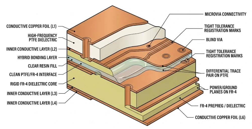
3. The Complexity of Hybrid Lamination (PTFE + FR-4)

For high-frequency RF and microwave applications (e.g., 77 GHz automotive radar), engineers require ultra-low-loss materials like PTFE (Teflon) from Rogers or Taconic. However, building a 12-layer board entirely out of PTFE is prohibitively expensive. The solution is Hybrid Lamination, where the critical RF outer layers use PTFE, and the inner structural layers use inexpensive FR-4.

The Engineering Challenge: PTFE and FR-4 have drastically different Coefficients of Thermal Expansion (CTE) and melt temperatures. If pressed together using standard FR-4 prepreg, the PTFE layer may delaminate or warp wildly during cooling.
The APTPCB Solution: We deploy specialized, low-loss thermoset bonding prepregs (such as Rogers RO4450F or Taconic fastRise 27) that are chemically formulated to adhere to both PTFE and FR-4. We engineer a highly customized, dual-ramp thermal press profile that respects the curing curves of both disparate material systems, ensuring a flat, reliable hybrid board.

4. Managing Board Warpage (Bow and Twist)

A PCB must be exceptionally flat to undergo SMT assembly; excessive warpage (bow and twist) will cause the pick-and-place machine to drop components inaccurately, or cause BGA solder joints to crack open during reflow. Warpage is almost entirely driven by asymmetrical lamination stack-ups.

As a rule of physics, a board must be symmetrical across its Z-axis center. If you place a solid 2 oz copper ground plane on Layer 2, but Layer 9 (its mirror opposite) only has sparse 1 oz signal traces, the board will curl like a potato chip as it cools down from the 200°C lamination press, because the heavy copper shrinks at a different rate than the resin. Our engineering team enforces strict DFM guidelines, often recommending "copper thieving" (adding non-functional copper pour to sparse areas) to balance the metal density and ensure your boards arrive perfectly flat.

Frequently Asked Questions

Multilayer Lamination & Stack-Up FAQ

What is the difference between a Core and a Prepreg?
A Core is a rigid piece of raw material consisting of fiberglass and fully cured (hardened) resin, with solid copper foil pre-bonded to both sides. A Prepreg (pre-impregnated) is a sheet of fiberglass coated with uncured, soft resin, and has no copper. During lamination under heat and pressure, the prepreg melts, acts as the glue to bond the rigid cores together, and then permanently hardens.
What is Sequential Lamination, and when is it required?
Sequential lamination involves pressing a PCB multiple times. Unlike single-press lamination (which bonds all layers at once and is suitable only for through-hole vias), sequential lamination builds the board outward in stages. We laminate the inner core, drill/plate it, add more prepreg/copper, and press it again. This process is strictly required for HDI boards featuring blind, buried, or stacked laser microvias.
Why does my board warp after manufacturing, and how do you prevent it?
Board warpage (bow and twist) occurs primarily due to asymmetric CTE (Coefficient of Thermal Expansion) forces during the cooling phase of lamination. If the copper density or dielectric thickness is unbalanced across the Z-axis center, the board will bend. We prevent this by enforcing strict stack-up symmetry, calculating copper density per layer, adding copper thieving where necessary, and utilizing controlled cool-down presses.
Can you laminate different material brands in the same stack-up?
Yes. This is called a Hybrid Stack-up and is highly common for cost reduction in RF and high-speed designs. We frequently bond Rogers RO4350B or Panasonic Megtron 6 signal layers to standard FR-4 structural cores. This requires specialized bonding prepregs and a customized thermal profile to ensure the different materials remain perfectly bonded and flat after cooling.
What happens if there is "resin starvation" during lamination?
Resin starvation occurs when there is not enough liquid resin in the melting prepreg to completely fill the etched gaps between thick copper traces. This leaves microscopic air voids inside the board. During SMT reflow, these air voids expand violently, causing the board to delaminate (blister). We mathematically calculate copper retention and prescribe high-resin prepregs to prevent this fatal defect.
How do you ensure layer-to-layer registration on a 32-layer board?
This is one of the most difficult tasks in PCB manufacturing. Every core layer shrinks slightly during imaging and etching. We apply non-linear scaling compensation to the artwork of each individual layer. Then, before pressing, our X-ray induction bonding system uses cameras to locate the actual fiducials on every core, optically align every core and melt-tack them together, ensuring sub-mil registration accuracy.
What prepreg glass styles do you offer?
We stock a wide variety of standard and spread-glass fabrics. Standard weaves include 106, 1080 (high resin for filling gaps), 2116 (standard structural), and 7628 (thick, low cost). For high-speed digital designs (PCIe Gen5, 56G PAM4) where fiber-weave skew must be eliminated, we offer spread-glass (flat-glass) styles such as 1035, 1067, and 1078.
Does the lamination process affect trace impedance?
Significantly. The final impedance of a trace is heavily dependent on the distance to its reference plane (the dielectric thickness). During lamination, prepreg shrinks as resin is squeezed out to fill copper gaps. The final pressed thickness will be thinner than the raw prepreg data sheet value. Our CAM engineers use Polar Si9000 software to calculate this exact "pressed thickness" to guarantee your ±5% impedance targets.
What is the maximum board thickness you can press?
For standard production, we routinely press boards up to 3.2 mm (125 mil). For advanced high-layer-count backplanes (30 to 64 layers), our heavy-duty hydraulic presses can accommodate total board thicknesses up to 8.0 mm (315 mil). Note that extreme thicknesses require high-aspect-ratio plating capabilities for through-hole vias.
How do you test lamination quality and reliability?
Post-lamination quality is verified through several methods. We perform physical microsection (cross-section) analysis to verify dielectric thickness and void-free encapsulation. We conduct thermal stress testing (solder float at 288°C for 10 seconds) to ensure no delamination occurs. For high-reliability defense/aerospace boards, we also offer IST (Interconnect Stress Test) and peel strength testing.

Global Manufacturing Reach

Precision Lamination Services for Global Innovators

From rigid-flex medical wearables in Europe to massive AI server backplanes in Silicon Valley, global engineering teams rely on APTPCB for flawless multilayer lamination and stack-up execution. Same-day DFM review keeps your project on track.

North America
USA · Canada · Mexico

Defense contractors, telecom OEMs, and Silicon Valley hardware startups rely on APTPCB for complex HDI sequential lamination and hybrid RF stack-ups.

HDI LaminationHybrid StacksDefense
Europe
Germany · UK · Sweden · France

Automotive Tier-1 suppliers in Munich, industrial automation giants, and medical device innovators source our heavily inspected, void-free high-layer boards.

AutomotiveMedical DevicesHigh-Layer
Asia-Pacific
Japan · South Korea · Taiwan · India

Smart home innovators and high-performance computing (HPC) server manufacturers across APAC utilize our automated press lines to secure high-yield mass production.

HPC ServersConsumer TechMass Scale
Israel & Middle East
Israel · UAE · Saudi Arabia

Aerospace, defense, and renewable energy programs in the region rely on our meticulous quality control, extreme heavy copper encapsulation, and polyimide pressing.

AerospaceHeavy CopperPolyimide

Validate Your Stack-Up Design Today

Share your complex Gerber files, desired layer count, material requirements, and impedance targets. Our CAM engineering team will return a comprehensive lamination profile, pressed-thickness calculation, and detailed quotation within one business day.