How to Accelerate Your PCB Project
Best Practices for Ensuring the Fastest Turnaround
While we control the manufacturing speed, the way a design is submitted can significantly impact the timeline. Here is a practical guide based on our experience processing thousands of quick-turn orders to ensure your project avoids administrative or engineering delays.
1. Submit a Complete Data Package
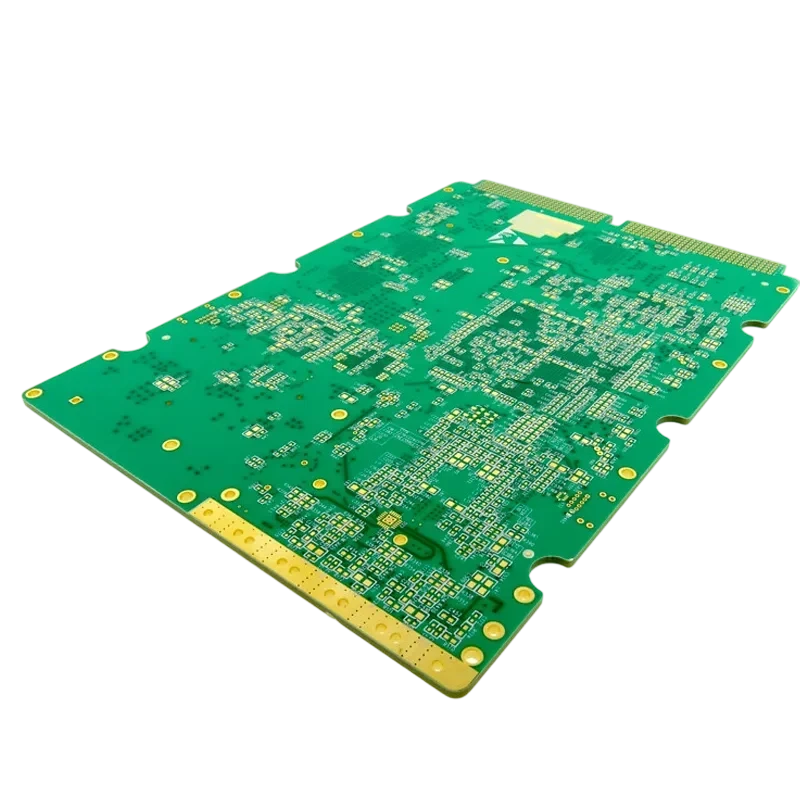
Missing files are the leading cause of "Day 1" delays. For bare boards, ensure your ZIP file includes all Gerber layers (RS-274X or ODB++), a complete NC Drill file, a clear fabrication drawing (showing board outline, dimensions, and layer stack-up), and an IPC-D-356 netlist. For PCBA, we additionally need a clean Bill of Materials (BOM) in Excel format with manufacturer part numbers, and a Centroid/Pick-and-Place (CPL) file. Teams that also include requirements for surface finish and quality documentation avoid the most common approval delays.
2. Design to Stocked Materials
If your project is highly time-sensitive, do not specify exotic or single-source laminates unless electrically necessary. For standard builds, specify "Isola 370HR or equivalent High-Tg FR-4." For high-speed or RF builds, utilize the materials we explicitly list as in-stock (e.g., Megtron 6, RO4350B, standard Aluminum MCPCB). If you mandate a rare material, procurement can add 5–15 days before fabrication even begins.
3. Provide Alternate Components on the BOM
In today's supply chain, a single $0.10 capacitor being out of stock can stall an entire assembly order. Review your BOM before submission and actively list approved alternates (Form-Fit-Function replacements) for passive components, standard logic ICs, and connectors. This empowers our procurement team to solve shortages instantly without pausing to email you for approval.
4. Avoid Unnecessary HDI (Microvias)
Laser-drilled blind and buried microvias require sequential lamination. Every lamination cycle (e.g., a 1+N+1 build) adds approximately 2 days to the manufacturing timeline due to the physics of pressing, curing, and re-drilling. If you can route your board using standard through-hole vias, your prototype will be manufactured significantly faster and at a lower cost.
5. Be Available for DFM Queries
When you submit a 48-hour turn order, our CAM engineers review it immediately. If we find an acid trap, a trace too close to the board edge, or an impedance mismatch, we will email you right away. Check your inbox frequently after submission! The 48-hour clock does not start until all engineering queries (EQs) are resolved and the final data is approved.