Scaling Guide
The Engineering Economics of PCB Mass Production
Transitioning from prototyping to mass production (typically defined as runs exceeding 5,000 to 10,000 units) is not merely about pressing a "print" button more times. It is a fundamental shift in manufacturing economics and process engineering. At APTPCB, we partner with hardware teams globally to restructure their designs for maximum yield and minimum unit cost. Below is a deep dive into the engineering strategies we apply to scale your hardware successfully.
1. Panelization and Material Utilization (Yield Optimization)
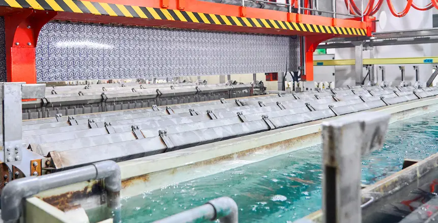
In a prototype run, the cost of the raw FR-4 material is negligible compared to the setup and engineering time. In mass production, material utilization becomes the primary cost driver. PCBs are manufactured on large, standard-sized laminates (e.g., 18" x 24" or 21" x 24"). If your single board design is arrayed (panelized) poorly, you might only utilize 60% of that standard sheet, throwing the remaining 40% in the trash—and paying for it.
Our CAM engineers perform rigorous Panelization Optimization. We calculate the exact array (e.g., a 2x3 or 4x4 matrix) that maximizes the usable area of the master laminate while still fitting perfectly onto our SMT pick-and-place conveyor belts. We strategically select between V-Cut scoring (best for straight, rectangular boards) and Tab-Routing with mouse-bites (best for irregular shapes) to ensure the boards remain perfectly rigid during component placement, yet easily snap apart (depanel) at final assembly without stressing the ceramic capacitors.
2. Tooling Amortization and Test Fixture Economics
Prototypes rely on slow, highly flexible machinery—like flying-probe electrical testers that move two robotic arms across the board to check continuity. Testing a complex board with a flying probe might take 3 minutes. If you build 50,000 boards, that equals 2,500 hours of testing time, which is economically ruinous.
For mass production, we invest in Hard Tooling. We manufacture custom "Bed-of-Nails" test fixtures—a physical jig embedded with hundreds of pogo pins that simultaneously contact every test point on your PCB array. A bed-of-nails fixture tests that same complex board in 3 seconds. While the fixture itself carries an upfront Non-Recurring Engineering (NRE) cost, it is quickly amortized across the volume run, drastically collapsing the per-unit testing cost.
3. DFM for High-Yield SMT Assembly
A board that is perfectly manufactured can still fail at mass production if it is not designed for automated assembly. Solder bridging, component tombstoning, and misaligned fine-pitch ICs can decimate your yield and skyrocket manual rework costs.
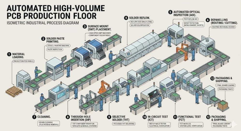
Before launching a volume PCBA run, our Design for Assembly (DFA) team scrutinizes the layout. We verify that all components have the correct thermal relief connections to ground planes (preventing cold solder joints), ensure proper spacing between tall components to avoid shadowing during wave soldering, and validate the inclusion of global and local fiducial marks. These high-contrast copper dots allow the vision systems of our multi-million-dollar Panasonic SMT machines to perfectly align the stencil and component placement heads at speeds exceeding 50,000 components per hour.
4. Supply Chain Elasticity and Component Procurement
The global electronics supply chain is volatile. A mass production run cannot afford to pause because a specific microcontroller or passive array is suddenly on a 52-week lead time. APTPCB acts as your strategic procurement partner.
We leverage our massive purchasing power and direct API integrations with global distributors (Digi-Key, Mouser, Arrow, Avnet) to lock in component allocations months in advance. We establish strategic safety stocks of your critical, long-lead-time ICs in our climate-controlled warehouse. For passive components (resistors, capacitors), we actively cross-reference your BOM to approve multiple reputable manufacturers (e.g., approving Murata, Yageo, and Samsung for a specific 100nF capacitor), ensuring that a localized shortage never stalls your global product rollout.
5. End-of-Line Quality and Traceability
For industries like automotive (IATF 16949) and medical (ISO 13485), mass production requires absolute traceability. If a single component fails in the field three years later, you must be able to trace it back to the exact manufacturing lot, the specific reel of components used, and the operator who ran the machine.
We implement serialized barcode tracking (laser etched or labeled) on every PCB panel. As the board moves through solder paste printing (SPI), automated optical inspection (AOI), reflow, and X-ray inspection, all quality data is tied to that serial number. This provides our clients with total transparency and an airtight defense against liability, ensuring your mass-produced hardware is as reliable as your engineering intent.