APTPCB Technical Whitepaper
Engineering Deep Dive: The Physics and Thermodynamics of PCB Drilling
For technical architects and lead hardware engineers, standard PCB definitions are inadequate. The following sections provide a rigorous technical breakdown of the material science, kinematics, and electromagnetic consequences of the PCB drilling process as executed at the APTPCB manufacturing facility.
1. The Physics of Signal Integrity and Backdrilling
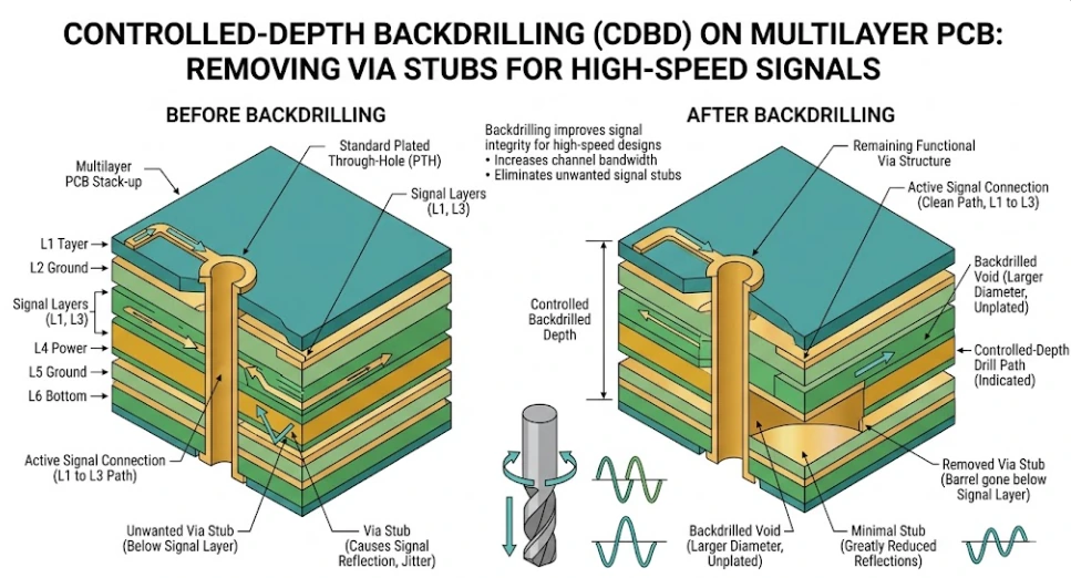
In high-speed digital design, a plated through-hole is not merely a DC connection but a complex capacitive and inductive network. When a signal transitions from Layer 1 to an internal stripline layer in a thick backplane, the remaining lower barrel becomes an unterminated transmission line, or via stub. This stub behaves as a quarter-wave resonator and can create a sharp null in the insertion-loss profile. Controlled-depth backdrilling removes that resonant structure and is often mandatory above 25G, 56G, and 112G signaling speeds.
2. Laser Microvia Ablation and Material Interaction
CO₂ Laser Thermodynamics: Operating in the infrared spectrum (~10.6 μm), the CO₂ laser transfers thermal energy to the molecular bonds of the epoxy resin, causing rapid vaporization. Because copper is highly reflective in the IR spectrum, the laser energy bounces off the internal copper target pad, preventing damage. This inherent "stop mechanism" makes CO₂ extremely fast and efficient for standard 1+N+1 HDI. However, the spot size of a CO₂ laser is limited by diffraction, making via diameters below 0.10 mm challenging.
UV Laser Photochemistry: Operating in the ultraviolet spectrum (~355 nm), UV lasers employ "cold ablation." The high-energy photons directly break the molecular bonds of both the dielectric polymer and the copper foil without inducing massive thermal gradients. This allows the UV laser to cut directly through the outer copper layer (Direct Laser Drilling, DLD), eliminating the need for a photolithographic window-opening step. Furthermore, the short wavelength allows for an exceptionally tight focal spot, enabling pristine 0.075 mm (3 mil) microvias with vertical sidewalls, an absolute necessity for 0.35 mm pitch BGA fan-out in Any-Layer ELIC configurations.
3. Desmear Chemistry and Plasma Activation
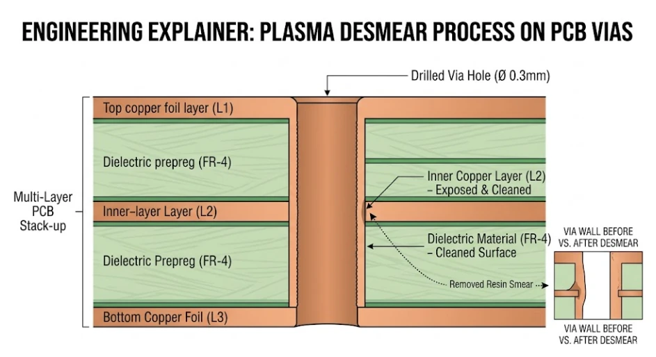
Mechanical drilling smears softened resin over exposed inner-layer copper, which must be removed before metallization. Standard FR-4 responds well to alkaline permanganate chemistries, while PTFE and other RF dielectrics require plasma activation. This is especially important in high-frequency PCB and mmWave designs, where poor hole-wall preparation directly compromises plating adhesion and long-term reliability.
PTFE/Teflon Laminates: Pure PTFE is soft and highly susceptible to thermal expansion. If the spindle speed (RPM) is too high or the feed rate (Infeed) is too slow, the drill bit dwells too long in the material, generating localized heat. The PTFE melts and smears across the hole, then immediately re-solidifies as a smooth, chemically inert barrier over the inner copper layers. To prevent catastrophic smearing, we utilize specialized "peck drilling" cycles, reduced RPM profiles, and aggressive chip loads to ensure the material is sheared and evacuated before thermal buildup can occur.
4. CAF Mitigation and Drill Bit Optimization
Conductive Anodic Filament (CAF) growth is a catastrophic electrochemical failure mode where copper ions migrate along the epoxy-glass interface from a high-voltage anode via to a cathode via, eventually causing an internal short circuit. As PCB designs become denser, the "web thickness" (the dielectric distance between two drilled hole walls) shrinks dangerously close to 0.15 mm.
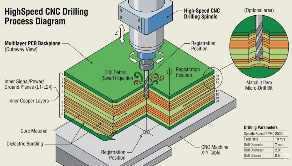
The drilling process is the primary mechanical trigger for CAF. If a dull drill bit is forced through the laminate, it fractures the silane bond between the woven glass fiber yarn and the surrounding epoxy resin. These micro-fractures create hollow capillary pathways. During operation in humid environments, moisture ingresses, dissolving the copper salts from the plating process, which then migrate under DC bias. APTPCB mitigates CAF mechanically by mandating high-frequency spindle run-out checks (Total Indicator Reading, TIR < 10 μm) to prevent bit wobble, utilizing aggressive feed rates to slice rather than push the glass bundles, and utilizing premium CAF-resistant high-Tg laminates with specialized silane treatments.
5. Electroplating Challenges in High-Aspect-Ratio Vias
Drilling a deep hole is only half the engineering challenge; depositing uniform copper inside that hole completes the interconnect. The Aspect Ratio (AR) is the ratio of the board thickness to the drilled hole diameter. An 8.0 mm thick backplane with a 0.5 mm hole has an AR of 16:1.
In a standard DC electroplating bath, the electric field density is heavily concentrated at the sharp edges of the hole entrance (the "dog bone" effect). Consequently, copper plates rapidly at the surface but very slowly in the center of the deep barrel. In a 15:1 hole, DC plating might deposit 40 μm of copper at the surface, but only 10 μm at the center—failing IPC Class 3 minimums and creating a critical weak point susceptible to cracking during the massive thermal shock of wave soldering.
APTPCB overcomes the laws of DC physics by utilizing Pulse-Reverse Electroplating. The rectifiers deliver a forward pulse (depositing copper), followed immediately by a high-current reverse pulse (anodic stripping). Because the electric field is strongest at the hole entrance, the reverse pulse preferentially strips the excess copper away from the surface edges while leaving the deep-barrel copper largely untouched. By continuously cycling this pulse-reverse waveform over several hours, we "push" the copper deep into the via, achieving exceptional throwing power and guaranteeing a uniform 20-25 μm copper barrel thickness from top to bottom, even in extreme 15:1 high-reliability aerospace backplanes.