1–67 GHZ READY

High-Frequency PCB Manufacturing — Rogers, PTFE, Hybrid Stackups

Rogers, PTFE, and hydrocarbon RF boards with cavity machining, ENEPIG/soft gold, and verified S-parameters up to mmWave keep antennas, radar, and telecom hardware on budget and on spec.

  • RO4350B / RO3003 / RT-duroid
  • Hybrid RF + FR-4 stackups
  • Cavity & waveguide machining
  • ENEPIG / soft gold finishes
  • ±5% impedance coupons
  • VNA reports to 40+ GHz

Get an Instant Quote

Full Quote →

High-Frequency PCB Fabrication & Assembly

APTPCB engineers translate RF requirements into Rogers/PTFE or hybrid stackups, balancing dielectric constant, dissipation factor, and copper roughness for antennas, radar, and high-frequency interconnects.

We manage cavity routing, plated-through slots, backdrill, and selective plating so launch geometry and ground references stay intact from prototype through volume.

Assembly support includes ENEPIG or soft gold, press-fit connectors, wire-bond prep, and fixture development with documented handling instructions for sensitive RF surfaces.

APTPCB's high-frequency reference defines HF boards as 500 MHz to 2 GHz and beyond, stressing the need to control insertion loss and impedance simultaneously. We reserve low-loss materials and EM simulation bandwidth for those microwave/millimeter-wave programs.

The reference catalog breaks down low-Dk/Df materials, stable CTE targets, and options such as Rogers, TMM, and F4B. We mirror that database in our stack-up library so antenna, radar, and satcom designs are matched quickly.

High-Frequency PCB Fabrication & Assembly

High-Frequency Programs Delivered

Examples across telecom radios, radar, SatCom terminals, automotive sensors, and test instrumentation.

5G/6G radio heads

5G/6G radio heads

Microwave backplanes

Microwave backplanes

Automotive radar modules

Automotive radar modules

Test & measurement analyzers

Test & measurement analyzers

SatCom terminals

SatCom terminals

RF sensor arrays

RF sensor arrays

RF Reliability & S-Parameter Compliance

Each build ships with impedance coupons, optional VNA sweeps, and documentation on plating thickness, cavity tolerances, and launch flatness.

Download Capabilities
Rogers / PTFEHybrid RF/FR-4Cavity machiningSoft gold / ENEPIGVNA to 40 GHzQuick-turn RF prototypes

APTPCB High-Frequency PCB Services

Full-stack RF fabrication covering material selection, stackup modeling, launch optimization, and post-build validation for microwave and mmWave hardware.

RF PCB Architectures

Single- or multi-layer PTFE, hybrid RF/FR-4, metal-backed RF, and rigid-flex RF harnesses.

  • Single-Layer PTFE – Microstrip antennas and power amplifiers on RT-duroid or RO3003.
  • Hybrid RF + FR-4 – Rogers cores for RF layers with FR-4 for control logic and power.
  • Metal-Backed RF – Aluminum or copper-backed PTFE for thermal spreading.
  • RF Rigid-Flex – Flex tails route RF signals in compact enclosures.
  • High-Layer Microwave – Multilayer stripline with balanced dielectric spacing for phased arrays.

RF Launch & Interconnect Features

  • Plated Through Slots: Maintain uniform impedance for edge launches and filters.
  • RF Vias & Fence Structures: Stitch grounds around antennas and cavities to contain energy.
  • Backdrilled RF Vias: Remove stubs that detune high-frequency lines.
  • Laser-Skived Cavities: Expose components while preserving dielectric surfaces.
  • Embedded Couplers: Precision etching for branchline and Lange couplers.

Sample RF Stackups

  • RO4350B 2-Layer: 0.508 mm core with 1 oz copper for L-band antennas.
  • Hybrid RO3003 + FR-4: PTFE outer layers for RF, FR-4 inner for control logic.
  • RT-duroid on Aluminum: 0.254 mm RT/duroid bonded to aluminum plate for PA modules.

Material & Design Guidelines

Match dielectric constant, thermal expansion, and copper roughness to frequency targets; keep stackups symmetrical for planarity.

  • Specify dielectric constant/tolerance and dissipation factor per layer.
  • Use rolled or very low profile copper for minimal loss.
  • Control copper plating and etch compensation for couplers and filters.
  • Document drill diameters and anti-pad rules for RF vias and grounds.

Reliability & RF Validation

RF builds undergo impedance verification, thermal cycling, and optional VNA/S-parameter testing up to 40+ GHz to ensure consistent performance.

Cost & Application Guidance

  • Hybrid stackups: Use RF materials only where necessary to manage cost.
  • Shared panelization: Combine small RF boards to reduce scrap.
  • Standardize finishes: ENIG for general RF, reserve soft gold for wire bond zones.

High-Frequency PCB Manufacturing Flow

1

Stackup & RF Review

Define materials, dielectric spacing, and launch geometry with RF engineers.

2

Imaging & Etch

LDI imaging with tight etch compensation for couplers and filters.

3

Cavity & Drill

Precision routing, plated slots, and via drilling with depth control.

4

Plating & Finish

Controlled copper plating, ENEPIG/soft gold, or silver as required.

5

Assembly & Integration

Cleanroom SMT, press-fit, or wire bond prep with carrier support.

6

RF Validation

Impedance coupons, VNA sweeps, and documentation ready for compliance.

7

Material Screening & Dielectric Control

Select low-Dk/low-Df laminates for the target band, then calibrate thickness tolerances and dielectric models to match simulation.

8

RF Validation & Process Convergence

Monitor insertion loss and impedance throughout imaging, etch, and finish; add TDR or VNA checkpoints whenever drift is detected.

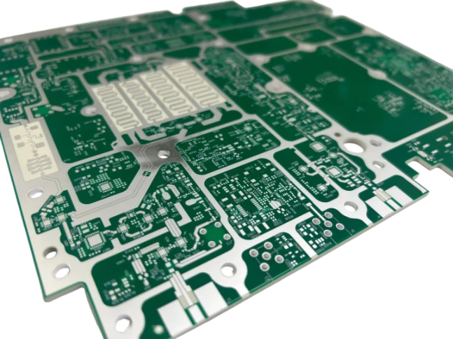
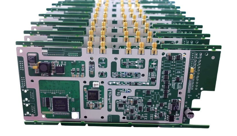
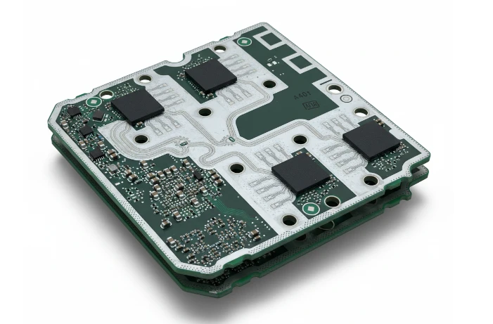
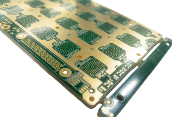
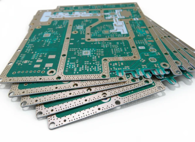
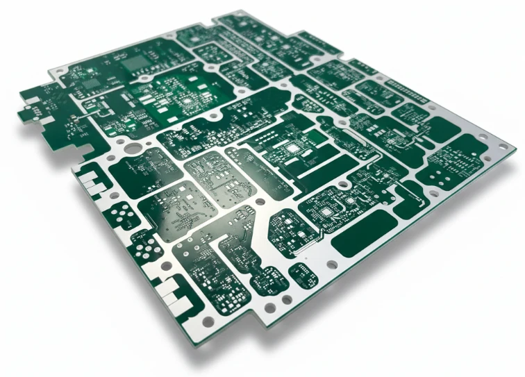
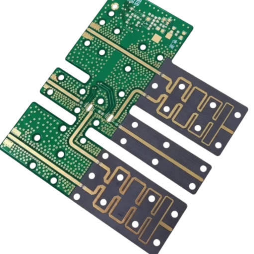
RF CAM & Stackup Engineering

CAM teams convert Gerber/ODB++ into RF-ready tooling, defining dielectric targets, cavity paths, and impedance coupons.

  • Confirm dielectric constants, tolerance, and copper roughness for each layer.
  • Define impedance coupons and RF launch references.
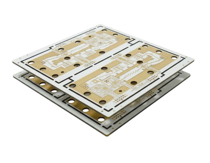
  • Plan cavity depths, plated slots, and keep-outs around antennas.
  • Schedule selective ENEPIG/soft gold for wire bond or probe pads.
  • Specify RF via stitching density and backdrill requirements.
  • Document handling/bake requirements for PTFE/ceramic materials.
  • Release fabrication notes covering surface cleanliness and packaging.

Manufacturing Execution & RF Feedback

Process engineers monitor etch, plating, and finish parameters, feeding RF test data back to design.

  • Track lamination temperature/pressure to avoid dielectric shift.
  • Verify etch line widths and copper thickness for couplers.
  • Inspect cavity depth, plated slot quality, and via walls.
  • Measure finish thickness (ENIG/soft gold) per spec.
  • Perform impedance/VNA tests on coupons; archive results.
  • Package boards with moisture control and protective films.
1–67 GHz

Frequency Window

RF, microwave, mmWave

Df ≤0.003

Dielectric Loss

Rogers/RT-duroid class materials

±5%

Impedance Control

Stripline & microstrip coupons

40+ GHz

VNA Testing

Documented S-parameters

Advantages of High-Frequency PCBs

Consistent RF performance, fast validation, and scalable production.

RF-Ready Materials

Certified Rogers/PTFE inventory with traceability.

Launch Precision

Cavity and slot machining maintain consistent impedance.

Test & Validation

Impedance + VNA data accompany every lot.

Hybrid Stackups

Mix RF materials with FR-4 to reduce cost.

Environmental Reliability

Thermal and humidity testing keep RF modules stable.

Faster NPI

Quick-turn RF protos with repeatable scaling paths.

Why Choose APTPCB?

Specialized materials, precision machining, and RF-focused testing keep loss, phase, and matching targets on track.

5G/6GRadarSatComAutomotive RFTest equipmentIoT gateways
APTPCB production line
RF line with Rogers

High-Frequency PCB Applications

From telecom radios to radar and instrumentation, RF boards power critical links.

Consistent stackups, controlled plating, and test data keep certification timelines short.

Telecom & Wireless

5G/6G radios, small cells, and microwave links.

RRUMassive MIMOBackhaulMicrowaveIoT hubs

Aerospace & Defense

Radar, EW, and SatCom payloads with tight RF specs.

RadarEWSatComAvionicsISR

Automotive & ADAS

Radar, V2X, and sensor modules with hybrid stackups.

LidarRadarV2XADASTelematics

Instrumentation & Test

Network analyzers, oscilloscopes, and RF testers.

VNASignal generatorsATEMetrologyInspection

IoT & Edge Devices

Gateways, smart meters, and RF sensor hubs.

IoTGatewaysSmart metersIndustrial RFSensors

Rigid-Flex RF

Wearables and aerospace harnesses blending RF and logic.

WearablesModulesEdge computeAerospace harnessMedical RF

Consumer Devices

Wi-Fi 6/6E routers, AR/VR, and connected devices.

Wi-Fi 6AR/VRSmart homeCPECameras

Medical & Life Sciences

Imaging probes and therapeutic RF applicators.

ImagingWearable therapyImplantsDiagnosticsMonitoring

High-Frequency Design Challenges & Solutions

RF designs demand disciplined materials, launch geometry, and process control to prevent detuning.

Common Design Challenges

01

Dielectric Variation

Improper material control shifts phase velocity and impedance.

02

Copper Roughness Loss

Rough copper increases conductor loss and phase noise.

03

Launch & Transition Errors

Misaligned cavities or slots detune edge launches.

04

Thermal Expansion Mismatch

Hybrid stackups crack or warp without matched CTE.

05

Surface Finish Impact

Incorrect plating thickness alters skin effect and bond quality.

06

Environmental Stability

Moisture uptake or handling scratches degrade RF performance.

Our Engineering Solutions

01

Material Traceability

Lot-based tracking and certs keep dielectric specs consistent.

02

Copper Roughness Control

Select VLP/HVLP foils and specify polishing where needed.

03

Precision Cavity Tooling

Laser/router programs hold tolerances for launches and filters.

04

Hybrid Stackup Modeling

Balance CTE and thickness to prevent warpage.

05

Surface Finish Governance

Targeted ENEPIG/soft gold thickness with SPC monitoring.

How to Control High-Frequency PCB Cost

RF materials and selective finishes are premium—reserve them for critical layers and pads. Reusing proven stackups and launch patterns shortens quoting and reduces NRE. Share frequency targets, power levels, and finish needs early so we can scope the simplest viable construction.

01 / 08

Hybridize Materials

Use Rogers/PTFE only on RF layers, FR-4 elsewhere.

02 / 08

Targeted Finishes

Apply soft gold only on bond pads; ENIG elsewhere.

03 / 08

Coordinate Connectors

Align SMA/SMPM cutouts with standard drill hits.

04 / 08

Standardize Launches

Reuse edge-launch geometries to avoid new tooling.

05 / 08

Panel Sharing

Combine small RF boards to maximize material usage.

06 / 08

Early RF DFx

Joint stackup reviews avoid respins and keep costs predictable.

07 / 08

Group Cavity Ops

Plan cavities and plated slots per panel to cut machine time.

08 / 08

Define Test Scope

Specify which lots need full VNA vs. sample validation.

Certifications & Standards

Quality, environmental, and industry credentials supporting reliable manufacturing.

Certification
ISO 9001:2015

Quality management for RF fabrication.

Certification
ISO 14001:2015

Environmental controls for PTFE handling.

Certification
ISO 13485:2016

Medical imaging RF assemblies.

Certification
IATF 16949

Automotive ADAS traceability.

Certification
AS9100 Rev D

Aerospace RF governance.

Certification
IPC-6012 / 6013

Class 3 rigid and rigid-flex acceptance.

Certification
UL 796 / UL94 V-0

Safety and flammability compliance.

Certification
RoHS / REACH

Material compliance for global shipments.

Selecting a High-Frequency PCB Partner

  • Rogers/PTFE inventory with certificates.
  • Cavity routing, plated slot, and laser drilling capability.
  • Selective ENEPIG/soft gold and wire-bond preparation.
  • VNA/S-parameter testing with documented fixtures.
  • Cleanroom SMT and press-fit connector experience.
  • Multilingual engineering support with 24-hour RF DFx feedback.
Selecting a High-Frequency PCB Partner

Quality & Cost Console

Process & Reliability Controls + Economic Levers

Unified dashboard connecting HDI quality checkpoints with the economic levers that compress cost.

Process & Reliability

Pre-Lamination Controls

Stack-Up Validation

  • Panel utilization+5–8%
  • Stack-up simulation±2% thickness
  • VIPPO planningPer lot
  • Material bake110 °C vacuum

Pre-Lamination Strategy

• Rotate outlines, mirror flex tails

• Share coupons across programs

• Reclaim 5-8% panel area

Registration

Laser & Metrology

Registration

  • Laser drill accuracy±12 μm
  • Microvia aspect ratio≤ 1:1
  • Coverlay alignment±0.05 mm
  • AOI overlaySPC logged

Laser Metrology

• Online laser capture

• ±0.05 mm tolerance band

• Auto-logged to SPC

Testing

Electrical & Reliability

Testing

  • Impedance & TDR±5% tolerance
  • Insertion lossLow-loss verified
  • Skew testingDifferential pairs
  • Microvia reliability> 1000 cycles

Electrical Test

• TDR coupons per panel

• IPC-6013 Class 3

• Force-resistance drift logged

Integration

Assembly Interfaces

Integration

  • Cleanroom SMTCarrier + ESD
  • Moisture control≤ 0.1% RH
  • Selective materialsLCP / low Df only where needed
  • ECN governanceVersion-controlled

Assembly Controls

• Nitrogen reflow

• Inline plasma clean

• 48h logistics consolidation

Architecture

Stack-Up Economics

Architecture

  • Lamination cyclesOptimize 1+N+1/2+N+2
  • Hybrid materialsLow-loss where required
  • Copper weightsMix 0.5/1 oz strategically
  • BOM alignmentStandard cores first

Cost Strategy

• Balance cost vs performance

• Standardize on common cores

• Low-loss only on RF layers

Microvia Planning

Via Strategy

Microvia Planning

  • Staggered over stacked-18% cost
  • Backdrill sharingCommon depths
  • Buried via reuseAcross nets
  • Fill specificationOnly for VIPPO

Via Cost Savings

• Avoid stacked microvias

• Share backdrill tools

• Minimize fill costs

Utilization

Panel Efficiency

Utilization

  • Outline rotation+4–6% yield
  • Shared couponsMulti-program
  • Coupon placementEdge pooled
  • Tooling commonalityPanel families

Panel Optimization

• Rotate for nesting efficiency

• Share test coupons

• Standardize tooling

Execution

Supply Chain & Coating

Execution

  • Material poolingMonthly ladder
  • Dual-source PPAPPre-qualified
  • Selective finishENIG / OSP mix
  • Logistics lanes48 h consolidation

Supply Chain Levers

• Pool low-loss material

• Dual-source laminates

• Match finish to need

High-Frequency PCB Manufacturing — Upload Data for RF Review

Talk to RF Engineers
IPC-6018 compliant builds
Rogers/PTFE expertise
Hybrid stackup guidance
RF validation included

Send stackups, dielectric targets, and finish needs—our RF team replies with DFx notes, costing, and test scope within one business day.

High-Frequency PCB FAQ

Material, finish, and validation answers for RF teams.