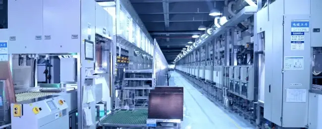
Unified Manufacturing
One Team Orchestrating High-Reliability PCB & PCBA Programs
APTPCB aligns multilayer PCB fabrication, turnkey assembly, and compliance support inside one manufacturing engine so engineering teams can launch faster with audit-ready evidence.
Get an Instant Quote
Precision Engineering
IPC Class 3 standards compliant. Advanced HDI and rigid-flex capabilities for mission-critical applications.
Rapid Scale-Up
Seamless transition from prototype to mass production. Automated assembly lines ensuring consistent quality.
Global Logistics
Optimized supply chain management. Worldwide shipping with real-time tracking and customs support.
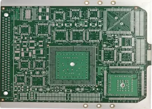
Engineered for Complexity.
Our core competencies across PCB manufacturing, PCBA assembly, and quality assurance—designed to handle the most demanding specifications in the industry.
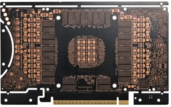
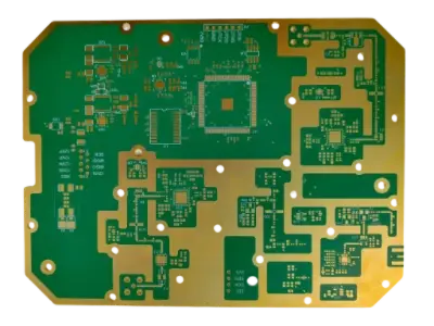
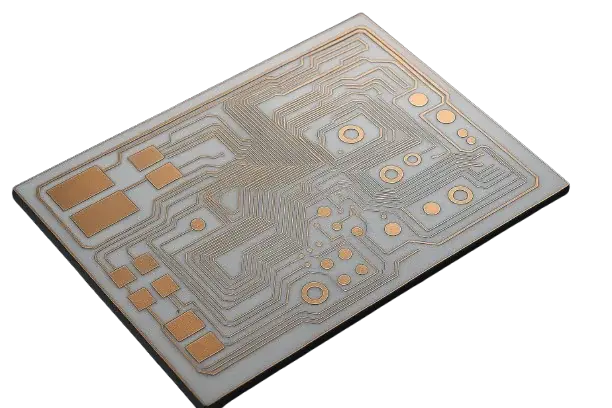
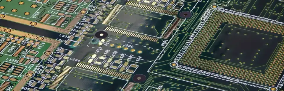
Advanced Fabrication Technology
High-End Product Types
Premium Materials
We partner with industry-leading material suppliers to ensure signal integrity and reliability.
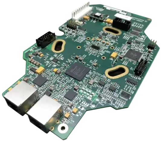
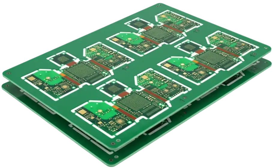
Seamless Turnkey Integration
PCB Design and Fabrication;Component Sourcing;PCB Assembly and Test
Testing & Quality
- • AOI & X-Ray Inspection
- • ICT (In-Circuit Test)
- • Functional Testing (FCT)
Engineering Capabilities
Pushing the boundaries of what's possible with cutting-edge manufacturing processes and materials.
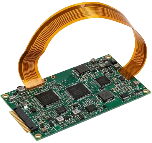
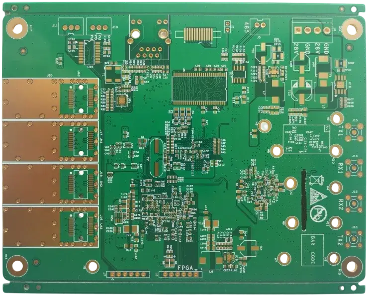
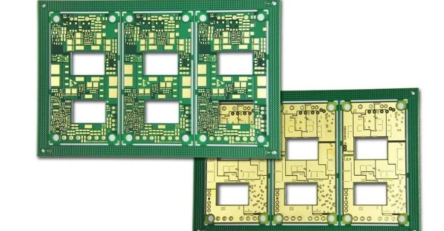
Rigid & Flex
- Up to 64 Layers (Rigid)
- Up to 12 Layers (Flex)
- Any-Layer HDI
- Staggered/Stacked Vias
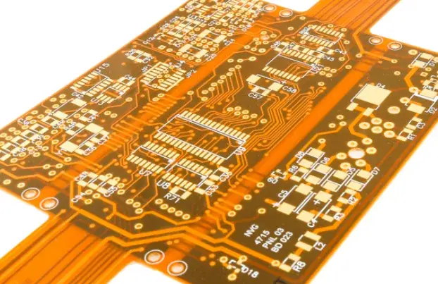
Flex PCB
- Dynamic Flex Stackups
- Adhesiveless Copper
- Coverlay Registration ≤35µm
- Bend Qualification
Metal PCB
- Aluminum / Copper Core
- >12 W/m·K Thermal Path
- Heavy Copper (up to 12oz)
- Embedded Coin
Ceramic PCB
- Alumina & AlN Substrates
- High Thermal Conductivity
- RF/Microwave Applications
- Extreme Reliability
Solutions Tuned to High-Growth Electronics Segments
Each industry path packages stackups, validation evidence, and compliance workflows so hardware teams can qualify with confidence.
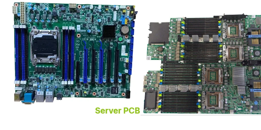
Server & Data Center
Backplanes, line cards, and accelerator modules with PAM4-ready channels.
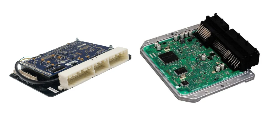
Automotive Electronics
ADAS controllers, BMS, and domain ECUs with IATF 16949 and PPAP coverage.
Medical Devices
Imaging, diagnostics, and wearable platforms ready for ISO 13485 alignment.
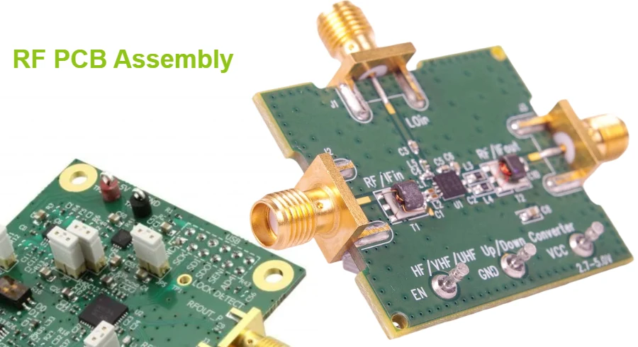
Communication Equipment
RF front ends, phased arrays, and satellite payloads with controlled impedance.
Aerospace & Defense
Mission-critical avionics, radar, and rugged electronics with traceable materials and environmental testing.
Industrial Control
PLCs, motion control, and IO modules built for 24/7 uptime in harsh environments.
Resources for Designers
Streamline your design-to-manufacturing workflow with our suite of free online tools, technical guides, and engineering resources.
Gerber Viewer
Instant online preview of your PCB files. Check layers, drills, and dimensions before fabrication.
Launch Tool →PCB Viewer
Interactive 3D visualization of PCB stackups and layer arrangements. Verify design before manufacturing.
View PCB →BOM Viewer
Analyze and validate your Bill of Materials. Check component availability and sourcing details.
View BOM →3D Viewer
Explore 3D models of your PCB and PCBA assemblies. Rotate, zoom, and inspect component placement.
View 3D →Circuit Simulator
Simulate circuit behavior and validate electrical performance before manufacturing.
Simulate →Impedance Calculator
Calculate trace width and spacing for controlled impedance stackups. Support for microstrip and stripline.
Calculate →Materials & Datasheets
Download material datasheets, design guidelines, and process capability notes for your projects.
Download →FAQ Hub
Find answers to common questions about PCB design, manufacturing, and assembly processes.
Browse FAQs →Engineering Blog
Read technical articles, case studies, and industry insights from our engineering team.
Read Blog →Ready to Scale?
Join the world's leading innovators who trust APTPCB with their most critical electronics.