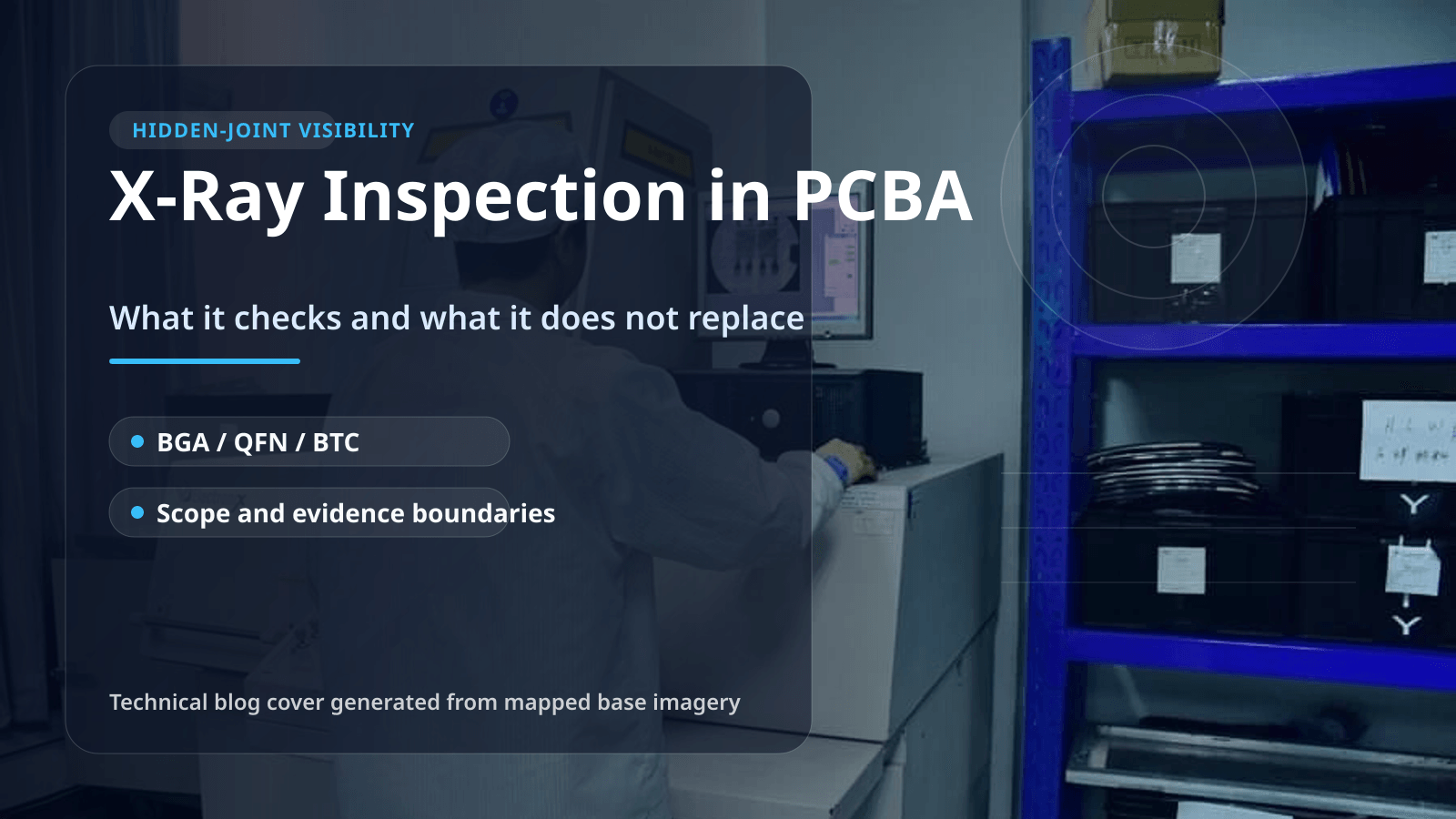
- X-ray inspection in PCBA should be treated as a hidden-joint and concealed-defect visibility layer, not as a generic statement that the whole board is fully verified.
- The strongest boundary is simple: AOI checks visible assembly features, X-ray checks concealed solder areas and hidden-joint questions, and electrical or functional test answer different questions later.
- A board can pass AOI and still need X-ray. A board can pass X-ray and still fail ICT, flying probe, or functional test.
- X-ray becomes more important when package geometry blocks optical visibility, especially under hidden-joint structures.
- X-ray should be discussed in terms of the concealed conditions it helps inspect and the evidence that still has to come from other gates.
Quick Answer X-ray inspection in PCBA is used when the assembly includes hidden or hard-to-see solder areas that cannot be evaluated confidently through surface optical inspection alone. It belongs in the quality stack as a concealed-defect inspection layer, especially around packages such as BGA or QFN families and other hidden-joint conditions. It does not replace AOI for visible defects, and it does not replace electrical or functional verification.
For the broader quality-stack view that connects SPI, AOI, X-ray, ICT, flying probe, functional test, and release gates, start with the PCBA Assembly Test and Quality Guide.
Table of Contents
- What should engineers review first?
- What does X-ray inspection in PCBA actually mean?
- What defect classes does X-ray really own?
- How does X-ray differ from AOI and electrical test?
- When does X-ray become more important in a build?
- What should be frozen before relying on X-ray results?
- Next steps with APTPCB
- FAQ
- Public references
- Author and review information
What should engineers review first?
Start with package visibility, hidden-joint risk, inspection stage, and downstream test dependency.
That order matters because X-ray is often described too broadly. Ask instead:
Which solder conditions are no longer visible through normal optical inspection, and what later evidence is still required even after they are inspected?
The first review questions should be:
- Does the assembly include package areas that AOI cannot inspect with confidence?
- Is the main concern hidden-joint or concealed-solder evidence rather than visible geometry?
- Does the board still need electrical or functional verification after X-ray?
- Is X-ray being used as one layer in the quality plan, or is it being overstated as a complete release claim?
| Review axis | What to check | Why it matters | What X-ray alone does not prove |
|---|---|---|---|
| Package visibility | Whether solder areas are concealed under package bodies or dense structures | Hidden areas are where X-ray adds real value | Visible assembly correctness |
| Hidden-joint risk | Whether the main concern is concealed solder integrity | Keeps X-ray aligned to the correct defect class | Powered behavior or full release confidence |
| Inspection stage | Where X-ray sits relative to AOI and later tests | Stage defines how the evidence will be used | That all earlier or later gates can be skipped |
| Downstream dependency | Which later gates still own electrical or functional proof | X-ray is one layer, not the whole quality stack | End-use performance by itself |
What does X-ray inspection in PCBA actually mean?
In this context, X-ray inspection in PCBA means using X-ray-based inspection to review solder conditions or structures that are not fully visible through surface optical methods.
That usually includes:
- hidden-joint package areas
- concealed solder regions
- internal or obscured assembly conditions that need non-surface visibility
It does not mean:
- visible component placement review in place of AOI
- assembled-board electrical fault screening in place of ICT or flying probe
- powered functional verification in place of FCT
- complete shipment release by itself
That boundary matters because the value of X-ray comes from seeing where surface inspection cannot see well enough, not from becoming a universal proof tool.
What defect classes does X-ray really own?
X-ray owns the defect questions that depend on concealed-joint or non-surface visibility.
| Defect class | Why X-ray is useful | What still may be needed later |
|---|---|---|
| Hidden-joint solder conditions | The solder area is not fully visible from the surface | Electrical test to confirm the board behaves electrically as intended |
| Concealed package-joint review | Dense or bottom-terminated structures reduce optical access | Functional validation if the product must also prove powered operation |
| Post-rework hidden-joint confirmation | Dense-package rework may still need concealed-joint evidence after repair | Release review and traceability as separate governance layers |
| Hidden-defect screening in dense-package regions | Surface appearance alone may not answer the defect question | AOI for visible defects outside the concealed area |
This is why X-ray should be framed as a visibility tool for hidden conditions, not as a synonym for overall quality assurance.
How does X-ray differ from AOI and electrical test?
X-ray becomes easier to explain when each method stays in its own role.
| Method | What it mainly answers | What it does not replace |
|---|---|---|
| AOI | Whether visible placement, polarity, geometry, and visible solder features look acceptable | Hidden-joint inspection or electrical verification |
| X-ray | Whether concealed solder areas and hidden joints need inspection evidence | Visible optical review, electrical fault screening, or functional proof |
| ICT or flying probe | Whether the assembled board has electrical faults such as opens, shorts, or component issues | Visible inspection or hidden-joint imaging |
| FCT | Whether the assembled board works in its intended powered context | Upstream defect localization or concealed-joint inspection |
That table matters because several common misreadings appear again and again:
- X-ray is treated as if it makes AOI unnecessary
- X-ray is treated as if it proves the board is electrically correct
- X-ray is treated as if it can replace functional test
- AOI and X-ray are described as interchangeable because both are inspection methods
Those claims are weak because they ignore the fact that each layer answers a different question.
A common hidden-joint failure chain starts when the package body conceals the solder condition and AOI still shows a clean surface result. Rework, voiding, bridging, or insufficient hidden-joint wetting can remain invisible at that stage, so the board moves forward under false confidence. X-ray is the point where that concealed defect becomes visible before later electrical or functional symptoms turn it into a much slower debug problem. If the board skips that visibility layer where it is needed, the defect may only show up later as intermittent behavior, electrical failure, or release delay after too much value has already been added.
Related reading:
When does X-ray become more important in a build?
X-ray matters more when optical visibility is no longer enough.
That usually includes:
- boards with hidden-joint package families
- assemblies where the critical solder area sits under the package body
- dense-package regions where surface review cannot answer the real defect question
- post-rework verification where concealed solder evidence still matters
X-ray also becomes more important when the team needs a clearer hidden-joint review path before the board moves to later electrical or functional gates.
The most dangerous false-confidence case appears on BTC and dense BGA builds that look visually clean from the outside. A QFN may show neat heel and toe fillets all around the package edge, and AOI will often return a clean pass because every visible optical feature appears acceptable. That result can be badly misleading. AOI cannot see through the package body. Under X-ray, the same board may reveal a center thermal pad with voiding large enough to cripple heat transfer, or a BGA core region where thermal stress has already created a small hidden bridge that never appears on the surface image. If that board is released on the strength of an AOI pass alone, the defect stays buried until the customer powers the product and the package is forced to dissipate real heat. At that point the apparently healthy assembly can run into localized overheating, thermal runaway, or field failure that should have been stopped at inspection. That is why X-ray is not an optional polish step for hidden-joint packages. It is the last physical barrier against a board that looks good on the outside and fails where no optical method could see.
At the same time, X-ray is not the whole story when:
- visible placement or polarity is still the main concern
- the board still needs electrical defect screening
- the product still needs powered functional validation
The governing rule is:
use X-ray where hidden visibility is the real problem, but do not ask it to certify risks that belong to optical, electrical, or functional layers.
What should be frozen before relying on X-ray results?
Before X-ray results are used as real release evidence, freeze:
- the package and hidden-joint assumptions that make X-ray necessary
- the inspection scope, including which concealed areas need evidence
- the relationship between AOI, X-ray, and later electrical or functional gates
- the post-rework inspection rule where dense-package recovery is involved
- the release boundary between hidden-joint inspection and final product proof
If those items are still moving, X-ray can still provide useful engineering evidence, but it should not be overstated as complete board validation.
FAQ
Can X-ray inspection prove a PCBA is fully tested?
No. X-ray proves only what the concealed-inspection layer is responsible for. Electrical, functional, and release questions still belong to other gates.
Is X-ray the same as AOI?
No. AOI checks visible assembly features. X-ray is used when the important solder area is concealed or not fully visible on the surface.
If a board passes X-ray, do I still need ICT or flying probe?
Sometimes yes. X-ray does not replace assembled-board electrical fault screening.
When is X-ray usually the better fit?
It is usually the better fit when hidden joints or concealed solder areas are the main concern and optical visibility is no longer enough.
What is the most common mistake in X-ray planning?
Treating X-ray as if it is a complete substitute for AOI, electrical test, and functional validation instead of one concealed-defect layer in a larger quality path.
Next steps with APTPCB
If your high-density PCBA carries expensive BGA devices, QFN power packages, or RF shields, and your team is still uncertain where the real voiding limit should be, how hidden-joint acceptance should be defined, or whether AOI is being trusted beyond its physical boundary, stop treating inspection planning as a documentation afterthought. This is where many builds still look clean on the surface while the real thermal and hidden-joint risk is already locked inside the assembly.
Send the BOM, assembly drawing, and Gerber package to sales@aptpcb.com or through the quote page.
APTPCB's NPI and quality-engineering team will return a Hidden-Joint & Inspection Strategy Review within 24 hours. We will help you set realistic voiding acceptance criteria, decide where AOI must hand off to X-ray, and balance X-ray, AOI, and electrical test coverage before you commit to expensive volume assembly with hidden defects still escaping the quality plan.
Public references
NASA Inspection and Quality Control Public inspection-program anchor for non-destructive analysis and quality-control workflow vocabulary.
IPC-A-610H Table of Contents Public standards anchor for workmanship context around electronic assemblies.
IPC J-STD-001J Table of Contents Public standards anchor for soldered assembly requirements context.
APTPCB X-Ray Inspection Support-page context for X-ray as the concealed-defect and hidden-joint inspection layer.
PCBA Assembly Test and Quality Guide Companion page for the broader inspection and test stack discussed in this guide.
Author and review information
- Author: APTPCB hidden-joint inspection content team
- Technical review: X-ray inspection and PCBA quality engineering team
- Last updated: 2026-05-13