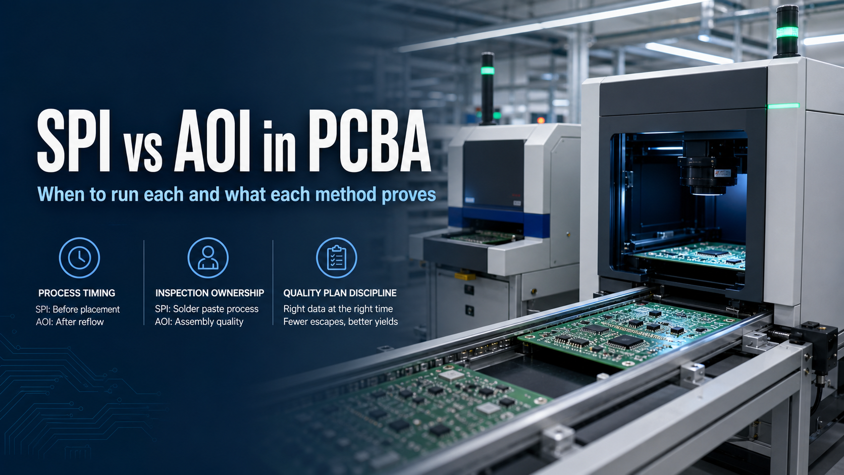
- SPI and AOI are both inspection methods, but they belong to different stages of the assembly flow.
- SPI belongs to solder paste control before placement and reflow. AOI belongs to visible assembly inspection around placement or after reflow.
- The key engineering boundary is not
SPI or AOI. It is what defect class is being checked at what stage. - A board can pass SPI and still fail AOI. A board can pass AOI and still fail X-ray, ICT, flying probe, or functional test.
- The safest planning model is to use SPI and AOI as separate layers inside a larger quality path rather than to collapse them into one generic inspection claim.
Quick Answer SPI should run when the team needs to confirm that solder paste deposition is under control before later assembly stages hide the printing result. AOI should run when the team needs optical evidence about visible placement, polarity, geometry, and visible solder features. They are not interchangeable methods. SPI answers a paste-process question before reflow; AOI answers a visible-assembly question later in the build flow.
For the broader inspection-and-test stack that connects SPI, AOI, X-ray, ICT, flying probe, functional test, and release gates, start with the PCBA Assembly Test and Quality Guide.
Table of Contents
- What should engineers review first?
- What does SPI actually check?
- What does AOI actually check?
- How do SPI and AOI differ in the build flow?
- When should a build rely more on SPI?
- When should a build rely more on AOI?
- What should be frozen before using either result as release evidence?
- Next steps with APTPCB
- FAQ
- Public references
- Author and review information
What should engineers review first?
Start with inspection stage, defect visibility, process risk, and downstream dependency.
That order matters because SPI vs AOI is often framed as if both methods are doing the same job. They are not.
The better question is:
Which defect class needs evidence first, and at what point in the assembly flow can that evidence still be trusted?
The first review questions should be:
- Is the main concern solder paste deposition before placement and reflow?
- Is the main concern visible component placement, polarity, geometry, or visible solder features?
- Are hidden-joint packages or electrical faults still going to require later gates?
- Is this build still in first-build learning, or is it already operating as a more stable repeat process?
| Review axis | What to check | Why it matters | What SPI or AOI alone does not prove |
|---|---|---|---|
| Inspection stage | Whether the check happens before reflow or after assembled features are visible | Stage determines what the system can actually inspect | Full board release confidence |
| Defect class | Whether the target problem is paste-related or visible assembly-related | Keeps the method aligned with the real risk | Hidden-joint integrity or powered behavior |
| Process risk | Whether the build is more likely to fail at print, placement, or later stages | Controls where early evidence is most valuable | That one inspection layer covers everything |
| Downstream dependency | Whether X-ray, electrical test, or FCT still owns later proof | Inspection is only part of the quality stack | That inspection alone makes later gates unnecessary |
What does SPI actually check?
SPI checks solder paste deposition before later stages of the SMT flow.
That makes SPI a process-control layer rather than a final assembled-board verdict.
In practical terms, SPI is used to look at whether paste printing appears to be under control before the board moves forward. That is why SPI belongs upstream of placement and reflow in the inspection sequence.
What SPI does not do:
- verify final component placement
- verify visible post-reflow assembly geometry
- inspect hidden joints after soldering
- prove assembled-board electrical behavior
This is the most common mistake in weak SPI articles: they describe SPI as if it proves assembly quality in general. It does not. It proves an earlier and narrower process question.
What does AOI actually check?
AOI checks visible assembly features.
That usually includes:
- component presence
- orientation and polarity
- placement shift or skew
- visible solder-feature issues
- some visible anomalies on the assembled board
AOI is strongest when the defect can be seen optically on the board surface.
What AOI does not do:
- prove solder paste was correct before reflow
- replace hidden-joint inspection under concealed packages
- replace electrical fault screening
- replace functional behavior validation
This is why AOI is best understood as a visible-defect screening layer, not as a blanket claim that the board has already been fully tested.
How do SPI and AOI differ in the build flow?
The stage split is the main point.
| Method | What it mainly answers | Where it sits | What it does not replace |
|---|---|---|---|
| SPI | Whether solder paste deposition is in control before later assembly stages | Before placement and reflow | AOI, X-ray, or electrical test |
| AOI | Whether visible placement, geometry, polarity, and solder features look acceptable | Around placement or after reflow, depending on the inspection plan | SPI, X-ray, or electrical test |
That means the relationship is not really SPI vs AOI in a winner-takes-all sense.
The relationship is:
- SPI catches an upstream process problem before it becomes a later assembly problem
- AOI screens the visible assembled result after placement or soldering has created something worth visually checking
The real failure chain starts when paste control is weak but the build is asked to rely on later inspection alone. Paste volume, offset, or bridging risk leaves the stencil stage without being corrected. Reflow then turns that print variation into visible solder defects, skewed parts, or bridges that AOI has to catch after the process window has already narrowed. If those visible defects survive or are misread, the problem can continue into electrical test or debug. That is why SPI and AOI are complementary. One controls the upstream print condition before it becomes a downstream assembly defect, and the other confirms what the assembled surface actually looks like after placement and reflow.
The cost difference becomes brutal on dense boards carrying 0.4 mm pitch BGA sites or QFN packages with large bottom thermal pads. A slightly clogged stencil aperture can quietly print insufficient paste volume onto one critical pad row. If SPI catches that defect before placement, the recovery path is almost trivial: wipe the bare board clean, reprint, and move on. The practical recovery cost is essentially $0 cost compared with any downstream repair. If the line skips SPI and waits for AOI to discover the result later, the defect is no longer a printing deviation. It has already been converted by reflow into an Open joint, a Tombstone, or another post-solder defect inside a crowded assembly zone. Now the only recovery path is Thermal rework on a finished board. That means labor, local reheating, process delay, and a real risk of Thermal trauma to nearby fine-pitch passives and already-stressed solder joints. This is why SPI is a preventive investment and AOI is a lagging indicator. They do not fail at the same cost level.
Related reading:
When should a build rely more on SPI?
SPI matters more when print quality is an early risk that the team wants to catch before placement and reflow hide it.
That usually includes:
- dense SMT builds
- fine-pitch or bottom-terminated package planning
- first-build learning where print stability is still being established
- assemblies where upstream paste-process control is an important predictor of later solder outcomes
In that role, SPI is valuable because it helps the team stop a printing problem before it grows into a more expensive downstream defect.
But the language still needs discipline:
SPI is an upstream process-control layer. It is not a substitute for later visible inspection, hidden-joint review, or board-level electrical verification.
When should a build rely more on AOI?
AOI matters more when visible assembly correctness is the main concern.
That often includes:
- placement confirmation
- polarity review
- visible geometry issues
- visible solder-feature anomalies
- repeat screening of visible defects before later test layers
AOI also becomes more important when the goal is to keep visible assembly defects from reaching X-ray, electrical test, or functional validation.
At the same time, AOI becomes less complete when:
- hidden-joint packages dominate the risk
- the main problem sits earlier in solder paste printing
- the main concern is electrical behavior rather than optical appearance
That is why AOI should be planned as a visible-inspection layer, not as a universal quality endpoint.
What should be frozen before using either result as release evidence?
Before SPI or AOI results are used as real release evidence, freeze:
- the assembly flow stage being inspected
- the defect classes each inspection step is expected to own
- the package-visibility assumptions, especially where hidden joints matter
- the later plan for X-ray, electrical test, or functional validation where required
- the release boundary between process control, visible inspection, and final shipment confidence
If those items are still moving, SPI and AOI can still provide useful process feedback, but their results should not be overstated as full product proof.
Next steps with APTPCB
If your dense PCBA is already suffering from high post-reflow rework rates, or your NPI team is still debating whether fine-pitch packages really justify mandatory SPI before mass build, the real question is not whether SPI sounds nice on paper. It is whether you want to catch a print defect at bare-board stage or pay for Thermal rework after the assembly has already absorbed heat, labor, and schedule risk.
Send the Gerber or ODB++ package, stencil intent, and BOM to sales@aptpcb.com or through the quote page.
APTPCB's SMT and quality-engineering team will return an SMT Process Control & Inspection Strategy Review within 24 hours. We will identify which package families must rely on SPI for paste-volume interception, which regions are better covered by AOI, and how to structure the inspection flow for the highest practical First-Pass Yield (FPY) before you commit the build to volume assembly.
FAQ
Is SPI the same as AOI?
No. SPI checks solder paste deposition before later SMT stages. AOI checks visible assembly features later in the process.
If a board passes SPI, can it still fail AOI?
Yes. A board can pass paste inspection and still develop visible placement or solder-related issues later.
If a board passes AOI, do I still need X-ray?
Sometimes yes. AOI does not replace hidden-joint inspection where concealed solder areas need evidence.
Can AOI replace ICT or flying probe?
No. AOI is an optical method. ICT and flying probe are electrical methods for different defect classes.
What is the biggest planning mistake in SPI vs AOI discussions?
Treating them as interchangeable inspection names instead of keeping the stage boundary and defect ownership clear.
Public references
Koh Young SPI Technology Public process-technology anchor for SPI as an upstream solder-paste inspection layer.
Koh Young AOI Technology Public process-technology anchor for AOI as a visible optical inspection layer.
IPC-A-610H Table of Contents Public standards anchor for visible assembly workmanship context.
PCBA Assembly Test and Quality Guide Companion page for the broader inspection-and-test stack used across this guide.
X-Ray Inspection in PCBA Companion page for the hidden-joint inspection boundary that neither SPI nor AOI replaces.
Author and review information
- Author: APTPCB PCBA inspection content team
- Technical review: SMT process control and inspection engineering team
- Last updated: 2026-05-13