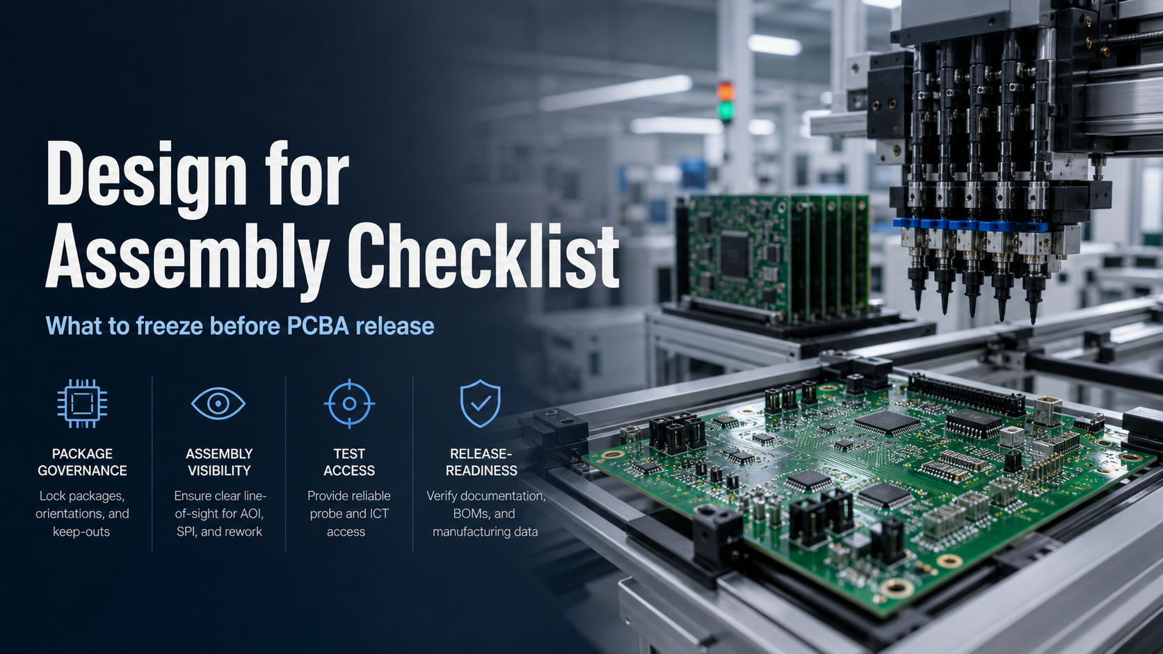
- A design for assembly checklist should be treated as a release-readiness review, not as a generic list of layout tips.
- The most useful boundary is to separate package and footprint governance, orientation discipline, process-route fit, inspection visibility, and test access.
- A board can be electrically complete and still be difficult to release if the assembly route, hidden-joint exposure, or documentation package remain unstable.
- A design for assembly checklist should explain what should be checked before first build and what should be frozen before the board enters a repeatable PCBA flow.
Quick Answer A design for assembly checklist is strongest when it reviews the board in order: package and footprint control, component-orientation discipline, mixed-process fit, inspection visibility, electrical-test access, and release-package alignment. Ask what still has to be cleaned up before the board can move into assembly, inspection, and first-build release without guesswork.
For the broader view of how assembly inputs connect to inspection, electrical verification, and shipment gates, start with the PCBA Assembly Test and Quality Guide.
Table of Contents
- What should engineers review first?
- What counts as DFA here?
- Which checklist areas expose release risk fastest?
- How do inspection and test planning connect to DFA?
- What should be frozen before RFQ, first build, or release?
- Next steps with APTPCB
- FAQ
- Public references
- Author and review information
What should engineers review first?
Start with footprint governance, orientation consistency, process-route fit, inspection visibility, and test-access readiness.
That order matters because DFA problems usually become expensive when they are discovered too late. If the board enters NPI with unstable package choices, unclear orientation logic, or unresolved access conflicts, the later inspection and test layers inherit work that should have been closed upstream.
The first engineering questions are usually:
- Do the package and footprint choices still match the intended component families cleanly?
- Are polarity and pin-1-sensitive parts documented and placed with enough consistency to support setup and review?
- Does the assembly route still fit the population mix, especially if SMT, THT, selective solder, or hidden-joint inspection all matter?
- Can AOI, X-ray, ICT, flying probe, or FCT be planned without fighting avoidable access or visibility conflicts?
- Is the release package aligned well enough that BOM, assembly drawing, and quality plan describe the same board state?
| Review boundary | What it answers | What it does not prove |
|---|---|---|
| Footprint governance | Whether the package library and intended parts still align cleanly | That exact geometry is universally valid for every substitute |
| Orientation consistency | Whether sensitive parts can be interpreted and reviewed without ambiguity | That the whole build package is already released |
| Process-route fit | Whether the population still matches the planned assembly flow | That every inspection or test gate is already closed |
| Inspection visibility | Whether visible and hidden-joint review can be planned sensibly | That powered behavior has been validated |
| Test access | Whether electrical verification can be planned with the current design posture | That the product is ready to ship |
What counts as DFA here?
Here, design for assembly checklist means the board-level readiness review that sits between layout completion and controlled PCBA release.
That includes:
- package-library and footprint review
- orientation and polarity discipline
- mixed SMT and THT route awareness
- hidden-joint and inspection-visibility awareness
- test-access review for later electrical or functional validation
- release-package alignment across BOM, drawing, and quality path
It does not mean:
- one universal list of spacing numbers for every board
- guaranteed yield or lead-time outcomes
- a claim that visual inspection alone is enough
- proof that system-level validation is finished
That boundary matters because many DFA articles drift into invented geometry tables or generic manufacturing slogans. The better explanation is more disciplined:
DFA is the point where the team checks whether the board, the package, and the planned assembly flow still fit each other before release.
Which checklist areas expose release risk fastest?
The release risk usually shows up first in the places where design intent and assembly reality diverge.
1. Package-library and footprint governance
The checklist should confirm that the board is still using package definitions that match the intended component set cleanly.
That means reviewing:
- package-family identity
- footprint ownership and revision discipline
- polarity or pin-1 visibility
- whether late alternates still fit the same assembly assumptions
If the package library is unstable, the rest of the DFA review becomes harder to trust.
2. Orientation discipline
Orientation-sensitive parts should not rely on tribal knowledge.
The checklist should ask whether:
- pin-1-sensitive parts remain obvious in the release package
- polarized components are easy to verify during setup and review
- the assembly drawing and placement package describe orientation consistently
One of the worst NPI failures starts in the CAD library before a single component is mounted. Engineers define a symmetric QFN or LGA footprint without following a proper Zero-Orientation rule such as IPC-7351 or IEC 61188-7, then hand the centroid file to the SMT line as if the rotation convention were self-evident. It is not. The CAD zero angle can be off by 90 degrees or 180 degrees from the default EIA-481 tape-and-reel orientation. The situation becomes lethal when the designer also hides the Pin 1 mark under the package body to save space, leaving no reliable top-side cue for setup or optical review. The pick-and-place machine then installs the device in the wrong rotation without hesitation. AOI sees a top surface that still looks perfectly symmetric and returns a False Pass. The first power-on event is where the mistake becomes visible. VCC and GND are now effectively crossed into a Dead short, internal current spikes instantly, and the silicon fails hard enough to start Vaporized wire bonds and visible smoke on the board. That is not a documentation error. It is a destroyed first article caused by weak orientation governance.
For the orientation layer, see SMT Component Polarity.
3. Mixed-process fit
Boards that combine dense SMT with connectors, terminals, or other through-hole hardware need a cleaner route review than a pure SMT board.
The checklist should ask:
- does the board still fit the planned SMT and THT flow?
- are selective or manual exceptions visible enough?
- does mixed-process handling change what should be frozen before first build?
For that route split, see Mixed Assembly Planning.
4. Inspection visibility
Inspection planning belongs inside DFA because some assembly risks are visible and some are not.
That boundary matters when:
- optical inspection is expected to catch visible orientation or placement issues
- hidden-joint packages push risk into X-ray review
- tall or dense neighborhoods reduce what the optical layer can confirm
5. Test-access readiness
Electrical-test planning should not be left until after the board is released if the design already creates access constraints.
The checklist should ask whether the design posture still supports:
- fixture-based ICT if the program later needs it
- fixture-free flying probe if the board is still changing
- functional-test access and programming expectations where applicable
| Checklist area | Why it matters | What goes wrong when it is ignored |
|---|---|---|
| Footprint governance | Keeps the physical implementation tied to the intended package family | Late uncertainty about what the board is actually designed to mount |
| Orientation discipline | Prevents ambiguity during setup, FAI, and troubleshooting | Reversed or disputed placement intent |
| Mixed-process fit | Keeps assembly-route assumptions realistic | Unexpected manual exceptions or process queries during NPI |
| Inspection visibility | Separates visible-risk review from hidden-joint review | Overstated confidence in what AOI can actually prove |
| Test access | Prevents late DFT conflict between layout and verification needs | Electrical-test planning becomes reactive instead of designed |
A typical DFA failure chain starts when the package looks routable in CAD but the assembly window is already too narrow in production terms. A footprint or placement choice leaves weak polarity visibility, poor optical access, or too little separation between dense SMT and later hand or selective operations. The board still reaches the line because the mismatch looks manageable on screen. Reflow, selective solder, or rework then has to operate inside that narrowed window, visible defects are harder to screen, and electrical-test access is forced into a workaround posture. The result is not one abstract DFA concern. It is bridging, rework churn, blocked inspection confidence, or release delay caused by a package-to-process mismatch that should have been frozen earlier.
How do inspection and test planning connect to DFA?
DFA is upstream of inspection and test, but it should anticipate their needs.
That means keeping the boundaries clear:
| Downstream layer | What it mainly answers | What DFA should do upstream |
|---|---|---|
| AOI | Whether visible placement and solder-related features can be screened optically | Preserve readable orientation and visible review intent |
| X-ray | Whether hidden joints or concealed structures need inspection evidence | Flag when hidden-joint risk changes the release posture |
| ICT or flying probe | Whether electrical defects can be screened with the chosen access model | Avoid preventable access conflicts |
| FCT | Whether the assembled board behaves correctly in powered context | Keep programming, connectors, and setup intent from becoming ambiguous |
The safer rule is:
DFA should reduce avoidable downstream ambiguity, not pretend that downstream verification is unnecessary.
Useful companion pages:
What should be frozen before RFQ, first build, or release?
Before serious RFQ, first build, or release, freeze:
- the package-library and footprint choices that define the assembly posture
- orientation and polarity interpretation for sensitive parts
- the assembly route assumptions for SMT, THT, selective, or other special branches
- the inspection and test boundary, especially where visible review, hidden-joint review, and electrical verification differ
- the alignment between BOM, assembly drawing, placement data, and quality-plan expectations
If those items are still moving, the design may still be functionally promising, but the assembly release package is not yet fully stable.
Next steps with APTPCB
If you are preparing a dense PCBA first build and you are not fully certain that your CAD rotation model matches the machine's orientation logic, that mixed-height neighborhoods will survive wave-solder shadowing, or that hidden-pin packages still leave AOI enough visibility to catch the real defect, do not wait for first power-on to discover the answer. That is the point where many boards still look release-ready on screen while the assembly package is already carrying a preventable burn-up risk.
Send the ODB++ or IPC-2581 release package, full BOM, and XY centroid data to sales@aptpcb.com or through the quote page.
APTPCB's NPI and DFA engineering team will return a DFA Physical & Orientation Review within 24 hours. We will identify CAD zero-angle conflicts, verify machine-mount compatibility for complex package families, and flag assembly conditions that can turn an orientation mistake into an expensive first-build failure before you energize a single vulnerable device.
If you need to go deeper before release, review:
FAQ
Is a DFA checklist only about component spacing?
No. It is a broader release-readiness review covering package control, orientation discipline, process-route fit, inspection visibility, and test-access planning.
Why does DFA need to care about inspection?
Because the design determines what later inspection layers can and cannot see easily. That affects how confidently visible and hidden-joint risks can be separated.
Does DFA replace DFT or test planning?
No. DFA should anticipate those needs and avoid preventable conflicts, but electrical and functional verification still have their own downstream ownership.
What makes a board fail DFA review most often?
Usually not one dramatic defect, but a package that is still unstable: footprint questions, mixed-process ambiguity, weak orientation visibility, or unresolved release-package drift.
When should DFA be treated as complete?
Only when the package, assembly route, and verification boundaries are stable enough that first build does not depend on guesswork.
Public references
[KiCad Library Convention] (https://klc.kicad.org/) Public CAD-library reference for controlled footprint-library construction and review discipline.
IEC 61188-7 Public standards metadata for zero-orientation and CAD-library construction language.
IPC-A-610H Table of Contents Public standards anchor for workmanship and visible-assembly acceptability context.
IPC J-STD-001J Table of Contents Public standards anchor for soldered electrical and electronic assembly requirements context.
PCBA Assembly Test and Quality Guide Companion page for the layered release-readiness model that connects inputs, inspection, electrical verification, and release gates.
Author and review information
- Author: APTPCB PCBA manufacturability and release-readiness content team
- Technical review: DFA, package-library, and NPI planning team
- Last updated: 2026-05-13